MC9S12E256VPVE Freescale Semiconductor, MC9S12E256VPVE Datasheet - Page 298
MC9S12E256VPVE
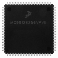
Manufacturer Part Number
MC9S12E256VPVE
Description
IC MCU 256K FLASH 25MHZ 112-LQFP
Manufacturer
Freescale Semiconductor
Series
HCS12r
Datasheet
1.MC9S12E256CFUE.pdf
(602 pages)
Specifications of MC9S12E256VPVE
Core Processor
HCS12
Core Size
16-Bit
Speed
25MHz
Connectivity
EBI/EMI, I²C, SCI, SPI
Peripherals
POR, PWM, WDT
Number Of I /o
91
Program Memory Size
256KB (256K x 8)
Program Memory Type
FLASH
Ram Size
16K x 8
Voltage - Supply (vcc/vdd)
2.35 V ~ 2.75 V
Data Converters
A/D 16x10b; D/A 2x8b
Oscillator Type
Internal
Operating Temperature
-40°C ~ 105°C
Package / Case
112-LQFP
Processor Series
S12E
Core
HCS12
Data Bus Width
16 bit
Data Ram Size
16 KB
Interface Type
I2C/SCI/SPI
Maximum Clock Frequency
50 MHz
Number Of Programmable I/os
92
Number Of Timers
12
Maximum Operating Temperature
+ 105 C
Mounting Style
SMD/SMT
3rd Party Development Tools
EWHCS12
Minimum Operating Temperature
- 40 C
On-chip Adc
16-ch x 10-bit
On-chip Dac
2-ch x 8-bit
For Use With
M68EVB912E128 - BOARD EVAL FOR MC9S12E128/64
Lead Free Status / RoHS Status
Lead free / RoHS Compliant
Eeprom Size
-
Lead Free Status / Rohs Status
Lead free / RoHS Compliant
Available stocks
Company
Part Number
Manufacturer
Quantity
Price
Company:

Part Number:
MC9S12E256VPVE
Manufacturer:
Freescale Semiconductor
Quantity:
10 000


Chapter 10 Inter-Integrated Circuit (IICV2)
10.1.3
The block diagram of the IIC module is shown in
10.2
The IICV2 module has two external pins.
10.2.1
This is the bidirectional serial clock line (SCL) of the module, compatible to the IIC bus specification.
10.2.2
This is the bidirectional serial data line (SDA) of the module, compatible to the IIC bus specification.
10.3
This section provides a detailed description of all memory and registers for the IIC module.
10.3.1
The memory map for the IIC module is given below in
the address offset.The total address for each register is the sum of the base address for the IIC module and
the address offset for each register.
298
External Signal Description
Memory Map and Register Definition
Block Diagram
IIC_SCL — Serial Clock Line Pin
IIC_SDA — Serial Data Line Pin
Module Memory Map
Interrupt
bus_clock
IIC
MC9S12E256 Data Sheet, Rev. 1.08
Registers
Figure 10-1. IIC Block Diagram
Clock
Control
Figure
Figure
Start
Stop
Arbitration
Control
Compare
Address
10-1.
In/Out
Data
Shift
Register
10-2. The address listed for each register is
Freescale Semiconductor
SCL
SDA
Related parts for MC9S12E256VPVE
Image
Part Number
Description
Manufacturer
Datasheet
Request
R

Part Number:
Description:
Manufacturer:
Freescale Semiconductor, Inc
Datasheet:
Part Number:
Description:
Manufacturer:
Freescale Semiconductor, Inc
Datasheet:
Part Number:
Description:
Manufacturer:
Freescale Semiconductor, Inc
Datasheet:
Part Number:
Description:
Manufacturer:
Freescale Semiconductor, Inc
Datasheet:
Part Number:
Description:
Manufacturer:
Freescale Semiconductor, Inc
Datasheet:
Part Number:
Description:
Manufacturer:
Freescale Semiconductor, Inc
Datasheet:
Part Number:
Description:
Manufacturer:
Freescale Semiconductor, Inc
Datasheet:
Part Number:
Description:
Manufacturer:
Freescale Semiconductor, Inc
Datasheet:
Part Number:
Description:
Manufacturer:
Freescale Semiconductor, Inc
Datasheet:
Part Number:
Description:
Manufacturer:
Freescale Semiconductor, Inc
Datasheet:
Part Number:
Description:
Manufacturer:
Freescale Semiconductor, Inc
Datasheet:
Part Number:
Description:
Manufacturer:
Freescale Semiconductor, Inc
Datasheet:
Part Number:
Description:
Manufacturer:
Freescale Semiconductor, Inc
Datasheet:
Part Number:
Description:
Manufacturer:
Freescale Semiconductor, Inc
Datasheet:
Part Number:
Description:
Manufacturer:
Freescale Semiconductor, Inc
Datasheet: