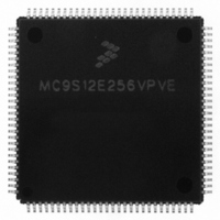
MC9S12E256VPVE Freescale Semiconductor, MC9S12E256VPVE Datasheet - Page 211

MC9S12E256VPVE
Manufacturer Part Number
MC9S12E256VPVE
Description
IC MCU 256K FLASH 25MHZ 112-LQFP
Manufacturer
Freescale Semiconductor
Series
HCS12r
Datasheet
1.MC9S12E256CFUE.pdf
(602 pages)
Specifications of MC9S12E256VPVE
Core Processor
HCS12
Core Size
16-Bit
Speed
25MHz
Connectivity
EBI/EMI, I²C, SCI, SPI
Peripherals
POR, PWM, WDT
Number Of I /o
91
Program Memory Size
256KB (256K x 8)
Program Memory Type
FLASH
Ram Size
16K x 8
Voltage - Supply (vcc/vdd)
2.35 V ~ 2.75 V
Data Converters
A/D 16x10b; D/A 2x8b
Oscillator Type
Internal
Operating Temperature
-40°C ~ 105°C
Package / Case
112-LQFP
Processor Series
S12E
Core
HCS12
Data Bus Width
16 bit
Data Ram Size
16 KB
Interface Type
I2C/SCI/SPI
Maximum Clock Frequency
50 MHz
Number Of Programmable I/os
92
Number Of Timers
12
Maximum Operating Temperature
+ 105 C
Mounting Style
SMD/SMT
3rd Party Development Tools
EWHCS12
Minimum Operating Temperature
- 40 C
On-chip Adc
16-ch x 10-bit
On-chip Dac
2-ch x 8-bit
For Use With
M68EVB912E128 - BOARD EVAL FOR MC9S12E128/64
Lead Free Status / RoHS Status
Lead free / RoHS Compliant
Eeprom Size
-
Lead Free Status / Rohs Status
Lead free / RoHS Compliant
Available stocks
Company
Part Number
Manufacturer
Quantity
Price
Company:
Part Number:
MC9S12E256VPVE
Manufacturer:
Freescale Semiconductor
Quantity:
10 000
- Current page: 211 of 602
- Download datasheet (4Mb)
6.3.2.2
Writes to this register will abort current conversion sequence but will not start a new sequence.
Read: Anytime
Write: Anytime
Freescale Semiconductor
ETRIGCH[3:0]
ETRIGSEL
Reset
Field
3:0
W
7
R
ETRIGSEL
ATD Control Register 1 (ATDCTL1)
0
7
External Trigger Source Select — This bit selects the external trigger source to be either one of the AD
channels or one of the ETRIG[3:0] inputs. See device specification for availability and connectivity of
ETRIG[3:0] inputs. If ETRIG[3:0] input option is not available, writing a 1 to ETRISEL only sets the bit but has
no effect, that means one of the AD channels (selected by ETRIGCH[3:0]) remains the source for external
trigger. The coding is summarized in
External Trigger Channel Select — These bits select one of the AD channels or one of the ETRIG[3:0] inputs
as source for the external trigger. The coding is summarized in
WRAP3
0
0
0
0
0
0
0
0
1
1
1
1
1
1
1
1
= Unimplemented or Reserved
0
0
6
WRAP2
Table 6-3. Multi-Channel Wrap Around Coding
Figure 6-4. ATD Control Register 1 (ATDCTL1)
0
0
0
0
1
1
1
1
0
0
0
0
1
1
1
1
Table 6-4. ATDCTL1 Field Descriptions
MC9S12E256 Data Sheet, Rev. 1.08
0
0
5
WRAP1
0
0
1
1
0
0
1
1
0
0
1
1
0
0
1
1
Table
WRAP0
6-5.
0
0
4
0
1
0
1
0
1
0
1
0
1
0
1
0
1
0
1
Description
ETRIGCH3
(MULT = 1) Wrap Around to AN0
Multiple Channel Conversions
Chapter 6 Analog-to-Digital Converter (ATD10B16CV4)
3
1
after Converting
Table
Reserved
ETRIGCH2
AN10
AN11
AN12
AN13
AN14
AN15
6-5.
AN1
AN2
AN3
AN4
AN5
AN6
AN7
AN8
AN9
1
2
ETRIGCH1
1
1
ETRIGCH0
1
0
211
Related parts for MC9S12E256VPVE
Image
Part Number
Description
Manufacturer
Datasheet
Request
R
Part Number:
Description:
Manufacturer:
Freescale Semiconductor, Inc
Datasheet:
Part Number:
Description:
Manufacturer:
Freescale Semiconductor, Inc
Datasheet:
Part Number:
Description:
Manufacturer:
Freescale Semiconductor, Inc
Datasheet:
Part Number:
Description:
Manufacturer:
Freescale Semiconductor, Inc
Datasheet:
Part Number:
Description:
Manufacturer:
Freescale Semiconductor, Inc
Datasheet:
Part Number:
Description:
Manufacturer:
Freescale Semiconductor, Inc
Datasheet:
Part Number:
Description:
Manufacturer:
Freescale Semiconductor, Inc
Datasheet:
Part Number:
Description:
Manufacturer:
Freescale Semiconductor, Inc
Datasheet:
Part Number:
Description:
Manufacturer:
Freescale Semiconductor, Inc
Datasheet:
Part Number:
Description:
Manufacturer:
Freescale Semiconductor, Inc
Datasheet:
Part Number:
Description:
Manufacturer:
Freescale Semiconductor, Inc
Datasheet:
Part Number:
Description:
Manufacturer:
Freescale Semiconductor, Inc
Datasheet:
Part Number:
Description:
Manufacturer:
Freescale Semiconductor, Inc
Datasheet:
Part Number:
Description:
Manufacturer:
Freescale Semiconductor, Inc
Datasheet:
Part Number:
Description:
Manufacturer:
Freescale Semiconductor, Inc
Datasheet:


