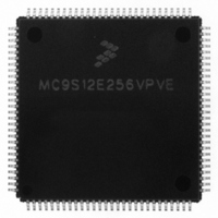
MC9S12E256VPVE Freescale Semiconductor, MC9S12E256VPVE Datasheet - Page 337

MC9S12E256VPVE
Manufacturer Part Number
MC9S12E256VPVE
Description
IC MCU 256K FLASH 25MHZ 112-LQFP
Manufacturer
Freescale Semiconductor
Series
HCS12r
Datasheet
1.MC9S12E256CFUE.pdf
(602 pages)
Specifications of MC9S12E256VPVE
Core Processor
HCS12
Core Size
16-Bit
Speed
25MHz
Connectivity
EBI/EMI, I²C, SCI, SPI
Peripherals
POR, PWM, WDT
Number Of I /o
91
Program Memory Size
256KB (256K x 8)
Program Memory Type
FLASH
Ram Size
16K x 8
Voltage - Supply (vcc/vdd)
2.35 V ~ 2.75 V
Data Converters
A/D 16x10b; D/A 2x8b
Oscillator Type
Internal
Operating Temperature
-40°C ~ 105°C
Package / Case
112-LQFP
Processor Series
S12E
Core
HCS12
Data Bus Width
16 bit
Data Ram Size
16 KB
Interface Type
I2C/SCI/SPI
Maximum Clock Frequency
50 MHz
Number Of Programmable I/os
92
Number Of Timers
12
Maximum Operating Temperature
+ 105 C
Mounting Style
SMD/SMT
3rd Party Development Tools
EWHCS12
Minimum Operating Temperature
- 40 C
On-chip Adc
16-ch x 10-bit
On-chip Dac
2-ch x 8-bit
For Use With
M68EVB912E128 - BOARD EVAL FOR MC9S12E128/64
Lead Free Status / RoHS Status
Lead free / RoHS Compliant
Eeprom Size
-
Lead Free Status / Rohs Status
Lead free / RoHS Compliant
Available stocks
Company
Part Number
Manufacturer
Quantity
Price
Company:
Part Number:
MC9S12E256VPVE
Manufacturer:
Freescale Semiconductor
Quantity:
10 000
- Current page: 337 of 602
- Download datasheet (4Mb)
Freescale Semiconductor
IPOLC
IPOLB
IPOLA
Field
2
1
0
Current Polarity — This buffered bit selects the PMF Value register for the PWM4 and PWM5 pins in top/bottom
software correction in complementary mode.
0 PMF Value 4 register in next PWM cycle.
1 PMF Value 5 register in next PWM cycle.
Note: The IPOLx bits take effect at the beginning of the next load cycle, regardless of the state of the load okay
Current Polarity — This buffered bit selects the PMF Value register for the PWM2 and PWM3 pins in top/bottom
software correction in complementary mode.
0 PMF Value 2 register in next PWM cycle.
1 PMF Value 3 register in next PWM cycle.
Note: The IPOLx bits take effect at the beginning of the next load cycle, regardless of the state of the load okay
Current Polarity — This buffered bit selects the PMF Value register for the PWM0 and PWM1 pins in top/bottom
software correction in complementary mode.
0 PMF Value 0 register in next PWM cycle.
1 PMF Value 1 register in next PWM cycle.
Note: The IPOLx bits take effect at the beginning of the next load cycle, regardless of the state of the load okay
1
2
3
The current status pins can be used as general purpose input/output ports.
The polarity of the ISx pin is latched when both the top and bottom PWMs are off. At the 0%
and 100% duty cycle boundaries, there is no deadtime, so no new current value is sensed.
Current is sensed even with 0% or 100% duty cycle.
ISENS
bit, LDOK. Select top/bottom software correction by writing 01 to the current select bits, ISENS[1:0], in the
PWM control register. Reading the IPOLx bits read the buffered value and not necessarily the value
currently in effect.
bit, LDOK. Select top/bottom software correction by writing 01 to the current select bits, ISENS[1:0], in the
PWM control register. Reading the IPOLx bits read the buffered value and not necessarily the value
currently in effect.
bit, LDOK. Select top/bottom software correction by writing 01 to the current select bits, ISENS[1:0], in the
PWM control register. Reading the IPOLx bits read the buffered value and not necessarily the value
currently in effect.
00
01
10
11
Table 11-17. PMFCCTL Field Descriptions (continued)
No correction
Manual correction
Current status sample correction on pins IS0, IS1, and IS2 during deadtime
Current status sample on pins IS0, IS1, and IS2
At the half cycle in center-aligned operation
At the end of the cycle in edge-aligned operation
Table 11-18. Correction Method Selection
MC9S12E256 Data Sheet, Rev. 1.08
1
Chapter 11 Pulse Width Modulator with Fault Protection (PMF15B6CV2)
Correction Method
Description
3
2
337
Related parts for MC9S12E256VPVE
Image
Part Number
Description
Manufacturer
Datasheet
Request
R
Part Number:
Description:
Manufacturer:
Freescale Semiconductor, Inc
Datasheet:
Part Number:
Description:
Manufacturer:
Freescale Semiconductor, Inc
Datasheet:
Part Number:
Description:
Manufacturer:
Freescale Semiconductor, Inc
Datasheet:
Part Number:
Description:
Manufacturer:
Freescale Semiconductor, Inc
Datasheet:
Part Number:
Description:
Manufacturer:
Freescale Semiconductor, Inc
Datasheet:
Part Number:
Description:
Manufacturer:
Freescale Semiconductor, Inc
Datasheet:
Part Number:
Description:
Manufacturer:
Freescale Semiconductor, Inc
Datasheet:
Part Number:
Description:
Manufacturer:
Freescale Semiconductor, Inc
Datasheet:
Part Number:
Description:
Manufacturer:
Freescale Semiconductor, Inc
Datasheet:
Part Number:
Description:
Manufacturer:
Freescale Semiconductor, Inc
Datasheet:
Part Number:
Description:
Manufacturer:
Freescale Semiconductor, Inc
Datasheet:
Part Number:
Description:
Manufacturer:
Freescale Semiconductor, Inc
Datasheet:
Part Number:
Description:
Manufacturer:
Freescale Semiconductor, Inc
Datasheet:
Part Number:
Description:
Manufacturer:
Freescale Semiconductor, Inc
Datasheet:
Part Number:
Description:
Manufacturer:
Freescale Semiconductor, Inc
Datasheet:


