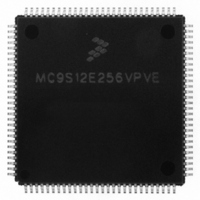
MC9S12E256VPVE Freescale Semiconductor, MC9S12E256VPVE Datasheet - Page 586

MC9S12E256VPVE
Manufacturer Part Number
MC9S12E256VPVE
Description
IC MCU 256K FLASH 25MHZ 112-LQFP
Manufacturer
Freescale Semiconductor
Series
HCS12r
Datasheet
1.MC9S12E256CFUE.pdf
(602 pages)
Specifications of MC9S12E256VPVE
Core Processor
HCS12
Core Size
16-Bit
Speed
25MHz
Connectivity
EBI/EMI, I²C, SCI, SPI
Peripherals
POR, PWM, WDT
Number Of I /o
91
Program Memory Size
256KB (256K x 8)
Program Memory Type
FLASH
Ram Size
16K x 8
Voltage - Supply (vcc/vdd)
2.35 V ~ 2.75 V
Data Converters
A/D 16x10b; D/A 2x8b
Oscillator Type
Internal
Operating Temperature
-40°C ~ 105°C
Package / Case
112-LQFP
Processor Series
S12E
Core
HCS12
Data Bus Width
16 bit
Data Ram Size
16 KB
Interface Type
I2C/SCI/SPI
Maximum Clock Frequency
50 MHz
Number Of Programmable I/os
92
Number Of Timers
12
Maximum Operating Temperature
+ 105 C
Mounting Style
SMD/SMT
3rd Party Development Tools
EWHCS12
Minimum Operating Temperature
- 40 C
On-chip Adc
16-ch x 10-bit
On-chip Dac
2-ch x 8-bit
For Use With
M68EVB912E128 - BOARD EVAL FOR MC9S12E128/64
Lead Free Status / RoHS Status
Lead free / RoHS Compliant
Eeprom Size
-
Lead Free Status / Rohs Status
Lead free / RoHS Compliant
Available stocks
Company
Part Number
Manufacturer
Quantity
Price
Company:
Part Number:
MC9S12E256VPVE
Manufacturer:
Freescale Semiconductor
Quantity:
10 000
- Current page: 586 of 602
- Download datasheet (4Mb)
1
2
Appendix A Electrical Characteristics
A.6.3
Three factors — source resistance, source capacitance and current injection — have an influence on the
accuracy of the ATD.
A.6.3.1
Due to the input pin leakage current as specified in
resistance there will be a voltage drop from the signal source to the ATD input. The maximum source
resistance R
If device or operating conditions are less than worst case or leakage-induced error is acceptable, larger
values of source resistance are allowed.
A.6.3.2
When sampling an additional internal capacitor is switched to the input. This can cause a voltage drop due
to charge sharing with the external and the pin capacitance. For a maximum sampling error of the input
voltage 1LSB, then the external filter capacitor, C
A.6.3.3
There are two cases to consider.
586
Conditions are shown in
Num C
The minimum time assumes a final sample period of 2 ATD clocks cycles while the maximum time assumes a final sample
period of 16 ATD clocks.
Reduced accuracy see
1
2
3
4
5
6
7
1. A current is injected into the channel being converted. The channel being stressed has conversion
D Reference Potential
C Differential Reference Voltage
D ATD Clock Frequency
D ATD 10-Bit Conversion Period
D ATD 8-Bit Conversion Period
D Recovery Time (V
P Reference Supply current
values of 0x3FF (0xFF in 8-bit mode) for analog inputs greater than VRH and 0x000 for values
less than VRL unless the current is higher than specified as disruptive conditions.
S
Factors Influencing Accuracy
Source Resistance
Source Capacitance
Current Injection
specifies results in an error of less than 1/2 LSB (2.5mV) at the maximum leakage current.
Conv, Time at 4.0MHz
Conv, Time at 2.0MHz ATD Clock f
Conv, Time at 2.0MHz ATD Clock f
Table A-4
Table A-22
DDA
=3.3 Volts)
Rating
unless otherwise noted; Supply Voltage 3.3V-10% <= V
Table A-20. 3.3V ATD Operating Characteristics
and
Table
2
MC9S12E256 Data Sheet, Rev. 1.08
ATD Clock f
A-23.
Clock Cycles
Clock Cycles
ATDCLK
ATDCLK
ATDCLK
High
Low
Table A-6
f
1
1
1024 * (C
N
V
T
T
Symbol
N
f
T
ATDCLK
RH
CONV10
CONV10
CONV10
CONV8
CONV8
t
V
I
V
REC
REF
RH
RL
-V
and
RL
Table A-7
INS
V
V
DDA
Min
- C
3.0
0.5
3.5
14
12
SSA
—
—
7
6
/2
INN
DDA
in conjunction with the source
).
<= 3.3V+10%
Typ
3.3
—
—
—
—
—
—
—
—
—
—
Freescale Semiconductor
V
0.250
V
Max
DDA
3.6
2.0
28
14
26
13
20
DDA
7
/2
Cycles
Cycles
MHz
Unit
mA
V
V
V
s
s
s
s
Related parts for MC9S12E256VPVE
Image
Part Number
Description
Manufacturer
Datasheet
Request
R
Part Number:
Description:
Manufacturer:
Freescale Semiconductor, Inc
Datasheet:
Part Number:
Description:
Manufacturer:
Freescale Semiconductor, Inc
Datasheet:
Part Number:
Description:
Manufacturer:
Freescale Semiconductor, Inc
Datasheet:
Part Number:
Description:
Manufacturer:
Freescale Semiconductor, Inc
Datasheet:
Part Number:
Description:
Manufacturer:
Freescale Semiconductor, Inc
Datasheet:
Part Number:
Description:
Manufacturer:
Freescale Semiconductor, Inc
Datasheet:
Part Number:
Description:
Manufacturer:
Freescale Semiconductor, Inc
Datasheet:
Part Number:
Description:
Manufacturer:
Freescale Semiconductor, Inc
Datasheet:
Part Number:
Description:
Manufacturer:
Freescale Semiconductor, Inc
Datasheet:
Part Number:
Description:
Manufacturer:
Freescale Semiconductor, Inc
Datasheet:
Part Number:
Description:
Manufacturer:
Freescale Semiconductor, Inc
Datasheet:
Part Number:
Description:
Manufacturer:
Freescale Semiconductor, Inc
Datasheet:
Part Number:
Description:
Manufacturer:
Freescale Semiconductor, Inc
Datasheet:
Part Number:
Description:
Manufacturer:
Freescale Semiconductor, Inc
Datasheet:
Part Number:
Description:
Manufacturer:
Freescale Semiconductor, Inc
Datasheet:


