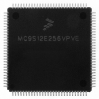
MC9S12E256VPVE Freescale Semiconductor, MC9S12E256VPVE Datasheet - Page 535

MC9S12E256VPVE
Manufacturer Part Number
MC9S12E256VPVE
Description
IC MCU 256K FLASH 25MHZ 112-LQFP
Manufacturer
Freescale Semiconductor
Series
HCS12r
Datasheet
1.MC9S12E256CFUE.pdf
(602 pages)
Specifications of MC9S12E256VPVE
Core Processor
HCS12
Core Size
16-Bit
Speed
25MHz
Connectivity
EBI/EMI, I²C, SCI, SPI
Peripherals
POR, PWM, WDT
Number Of I /o
91
Program Memory Size
256KB (256K x 8)
Program Memory Type
FLASH
Ram Size
16K x 8
Voltage - Supply (vcc/vdd)
2.35 V ~ 2.75 V
Data Converters
A/D 16x10b; D/A 2x8b
Oscillator Type
Internal
Operating Temperature
-40°C ~ 105°C
Package / Case
112-LQFP
Processor Series
S12E
Core
HCS12
Data Bus Width
16 bit
Data Ram Size
16 KB
Interface Type
I2C/SCI/SPI
Maximum Clock Frequency
50 MHz
Number Of Programmable I/os
92
Number Of Timers
12
Maximum Operating Temperature
+ 105 C
Mounting Style
SMD/SMT
3rd Party Development Tools
EWHCS12
Minimum Operating Temperature
- 40 C
On-chip Adc
16-ch x 10-bit
On-chip Dac
2-ch x 8-bit
For Use With
M68EVB912E128 - BOARD EVAL FOR MC9S12E128/64
Lead Free Status / RoHS Status
Lead free / RoHS Compliant
Eeprom Size
-
Lead Free Status / Rohs Status
Lead free / RoHS Compliant
Available stocks
Company
Part Number
Manufacturer
Quantity
Price
Company:
Part Number:
MC9S12E256VPVE
Manufacturer:
Freescale Semiconductor
Quantity:
10 000
- Current page: 535 of 602
- Download datasheet (4Mb)
18.4.3.1
These modes provide three operating configurations. Background debug is available in all three modes,
but must first be enabled for some operations by means of a BDM background command, then activated.
18.4.3.1.1
There is no external expansion bus in this mode. All pins of Ports A, B and E are configured as general
purpose I/O pins Port E bits 1 and 0 are available as general purpose input only pins with internal pull
resistors enabled. All other pins of Port E are bidirectional I/O pins that are initially configured as
high-impedance inputs with internal pull resistors enabled. Ports A and B are configured as
high-impedance inputs with their internal pull resistors disabled.
The pins associated with Port E bits 6, 5, 3, and 2 cannot be configured for their alternate functions IPIPE1,
IPIPE0, LSTRB, and R/W while the MCU is in single chip modes. In single chip modes, the associated
control bits PIPOE, LSTRE, and RDWE are reset to zero. Writing the opposite state into them in single
chip mode does not change the operation of the associated Port E pins.
In normal single chip mode, the MODE register is writable one time. This allows a user program to change
the bus mode to narrow or wide expanded mode and/or turn on visibility of internal accesses.
Port E, bit 4 can be configured for a free-running E clock output by clearing NECLK=0. Typically the only
use for an E clock output while the MCU is in single chip modes would be to get a constant speed clock
for use in the external application system.
18.4.3.1.2
In expanded wide modes, Ports A and B are configured as a 16-bit multiplexed address and data bus and
Port E bit 4 is configured as the E clock output signal. These signals allow external memory and peripheral
devices to be interfaced to the MCU.
Port E pins other than PE4/ECLK are configured as general purpose I/O pins (initially high-impedance
inputs with internal pull resistors enabled). Control bits PIPOE, NECLK, LSTRE, and RDWE in the
PEAR register can be used to configure Port E pins to act as bus control outputs instead of general purpose
I/O pins.
It is possible to enable the pipe status signals on Port E bits 6 and 5 by setting the PIPOE bit in PEAR, but
it would be unusual to do so in this mode. Development systems where pipe status signals are monitored
would typically use the special variation of this mode.
The Port E bit 2 pin can be reconfigured as the R/W bus control signal by writing “1” to the RDWE bit in
PEAR. If the expanded system includes external devices that can be written, such as RAM, the RDWE bit
would need to be set before any attempt to write to an external location. If there are no writable resources
in the external system, PE2 can be left as a general purpose I/O pin.
The Port E bit 3 pin can be reconfigured as the LSTRB bus control signal by writing “1” to the LSTRE bit
in PEAR. The default condition of this pin is a general purpose input because the LSTRB function is not
needed in all expanded wide applications.
Freescale Semiconductor
Normal Operating Modes
Normal Single-Chip Mode
Normal Expanded Wide Mode
MC9S12E256 Data Sheet, Rev. 1.08
Chapter 18 Multiplexed External Bus Interface (MEBIV3)
535
Related parts for MC9S12E256VPVE
Image
Part Number
Description
Manufacturer
Datasheet
Request
R
Part Number:
Description:
Manufacturer:
Freescale Semiconductor, Inc
Datasheet:
Part Number:
Description:
Manufacturer:
Freescale Semiconductor, Inc
Datasheet:
Part Number:
Description:
Manufacturer:
Freescale Semiconductor, Inc
Datasheet:
Part Number:
Description:
Manufacturer:
Freescale Semiconductor, Inc
Datasheet:
Part Number:
Description:
Manufacturer:
Freescale Semiconductor, Inc
Datasheet:
Part Number:
Description:
Manufacturer:
Freescale Semiconductor, Inc
Datasheet:
Part Number:
Description:
Manufacturer:
Freescale Semiconductor, Inc
Datasheet:
Part Number:
Description:
Manufacturer:
Freescale Semiconductor, Inc
Datasheet:
Part Number:
Description:
Manufacturer:
Freescale Semiconductor, Inc
Datasheet:
Part Number:
Description:
Manufacturer:
Freescale Semiconductor, Inc
Datasheet:
Part Number:
Description:
Manufacturer:
Freescale Semiconductor, Inc
Datasheet:
Part Number:
Description:
Manufacturer:
Freescale Semiconductor, Inc
Datasheet:
Part Number:
Description:
Manufacturer:
Freescale Semiconductor, Inc
Datasheet:
Part Number:
Description:
Manufacturer:
Freescale Semiconductor, Inc
Datasheet:
Part Number:
Description:
Manufacturer:
Freescale Semiconductor, Inc
Datasheet:


