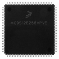
MC9S12E256VPVE Freescale Semiconductor, MC9S12E256VPVE Datasheet - Page 384

MC9S12E256VPVE
Manufacturer Part Number
MC9S12E256VPVE
Description
IC MCU 256K FLASH 25MHZ 112-LQFP
Manufacturer
Freescale Semiconductor
Series
HCS12r
Datasheet
1.MC9S12E256CFUE.pdf
(602 pages)
Specifications of MC9S12E256VPVE
Core Processor
HCS12
Core Size
16-Bit
Speed
25MHz
Connectivity
EBI/EMI, I²C, SCI, SPI
Peripherals
POR, PWM, WDT
Number Of I /o
91
Program Memory Size
256KB (256K x 8)
Program Memory Type
FLASH
Ram Size
16K x 8
Voltage - Supply (vcc/vdd)
2.35 V ~ 2.75 V
Data Converters
A/D 16x10b; D/A 2x8b
Oscillator Type
Internal
Operating Temperature
-40°C ~ 105°C
Package / Case
112-LQFP
Processor Series
S12E
Core
HCS12
Data Bus Width
16 bit
Data Ram Size
16 KB
Interface Type
I2C/SCI/SPI
Maximum Clock Frequency
50 MHz
Number Of Programmable I/os
92
Number Of Timers
12
Maximum Operating Temperature
+ 105 C
Mounting Style
SMD/SMT
3rd Party Development Tools
EWHCS12
Minimum Operating Temperature
- 40 C
On-chip Adc
16-ch x 10-bit
On-chip Dac
2-ch x 8-bit
For Use With
M68EVB912E128 - BOARD EVAL FOR MC9S12E128/64
Lead Free Status / RoHS Status
Lead free / RoHS Compliant
Eeprom Size
-
Lead Free Status / Rohs Status
Lead free / RoHS Compliant
Available stocks
Company
Part Number
Manufacturer
Quantity
Price
Company:
Part Number:
MC9S12E256VPVE
Manufacturer:
Freescale Semiconductor
Quantity:
10 000
- Current page: 384 of 602
- Download datasheet (4Mb)
Chapter 12 Pulse-Width Modulator (PWM8B6CV1)
12.3.2.2
The starting polarity of each PWM channel waveform is determined by the associated PPOLx bit in the
PWMPOL register. If the polarity bit is 1, the PWM channel output is high at the beginning of the cycle
and then goes low when the duty count is reached. Conversely, if the polarity bit is 0 the output starts low
and then goes high when the duty count is reached.
Read: anytime
Write: anytime
384
PWME1
PWME0
PPOL5
PPOL4
PPOL3
Reset
Field
Field
1
0
5
4
3
W
R
Pulse Width Channel 1 Enable
0 Pulse width channel 1 is disabled.
1 Pulse width channel 1 is enabled. The pulse modulated signal becomes available at PWM, output bit 1 when
Pulse Width Channel 0 Enable
0 Pulse width channel 0 is disabled.
1 Pulse width channel 0 is enabled. The pulse modulated signal becomes available at PWM, output bit 0 when
Pulse Width Channel 5 Polarity
0 PWM channel 5 output is low at the beginning of the period, then goes high when the duty count is reached.
1 PWM channel 5 output is high at the beginning of the period, then goes low when the duty count is reached.
Pulse Width Channel 4 Polarity
0 PWM channel 4 output is low at the beginning of the period, then goes high when the duty count is reached.
1 PWM channel 4 output is high at the beginning of the period, then goes low when the duty count is reached.
Pulse Width Channel 3 Polarity
0 PWM channel 3 output is low at the beginning of the period, then goes high when the duty count is reached.
1 PWM channel 3 output is high at the beginning of the period, then goes low when the duty count is reached.
PWM Polarity Register (PWMPOL)
0
0
7
its clock source begins its next cycle.
its clock source begins its next cycle. If CON01 = 1, then bit has no effect and PWM output line 0 is disabled.
PPOLx register bits can be written anytime. If the polarity is changed while
a PWM signal is being generated, a truncated or stretched pulse can occur
during the transition
= Unimplemented or Reserved
0
0
6
Table 12-2. PWME Field Descriptions (continued)
Figure 12-4. PWM Polarity Register (PWMPOL)
Table 12-3. PWMPOL Field Descriptions
PPOL5
MC9S12E256 Data Sheet, Rev. 1.08
0
5
PPOL4
NOTE
0
4
Description
Description
PPOL3
3
0
PPOL2
0
2
PPOL1
Freescale Semiconductor
0
1
PPOL0
0
0
Related parts for MC9S12E256VPVE
Image
Part Number
Description
Manufacturer
Datasheet
Request
R
Part Number:
Description:
Manufacturer:
Freescale Semiconductor, Inc
Datasheet:
Part Number:
Description:
Manufacturer:
Freescale Semiconductor, Inc
Datasheet:
Part Number:
Description:
Manufacturer:
Freescale Semiconductor, Inc
Datasheet:
Part Number:
Description:
Manufacturer:
Freescale Semiconductor, Inc
Datasheet:
Part Number:
Description:
Manufacturer:
Freescale Semiconductor, Inc
Datasheet:
Part Number:
Description:
Manufacturer:
Freescale Semiconductor, Inc
Datasheet:
Part Number:
Description:
Manufacturer:
Freescale Semiconductor, Inc
Datasheet:
Part Number:
Description:
Manufacturer:
Freescale Semiconductor, Inc
Datasheet:
Part Number:
Description:
Manufacturer:
Freescale Semiconductor, Inc
Datasheet:
Part Number:
Description:
Manufacturer:
Freescale Semiconductor, Inc
Datasheet:
Part Number:
Description:
Manufacturer:
Freescale Semiconductor, Inc
Datasheet:
Part Number:
Description:
Manufacturer:
Freescale Semiconductor, Inc
Datasheet:
Part Number:
Description:
Manufacturer:
Freescale Semiconductor, Inc
Datasheet:
Part Number:
Description:
Manufacturer:
Freescale Semiconductor, Inc
Datasheet:
Part Number:
Description:
Manufacturer:
Freescale Semiconductor, Inc
Datasheet:


