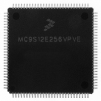
MC9S12E256VPVE Freescale Semiconductor, MC9S12E256VPVE Datasheet - Page 374

MC9S12E256VPVE
Manufacturer Part Number
MC9S12E256VPVE
Description
IC MCU 256K FLASH 25MHZ 112-LQFP
Manufacturer
Freescale Semiconductor
Series
HCS12r
Datasheet
1.MC9S12E256CFUE.pdf
(602 pages)
Specifications of MC9S12E256VPVE
Core Processor
HCS12
Core Size
16-Bit
Speed
25MHz
Connectivity
EBI/EMI, I²C, SCI, SPI
Peripherals
POR, PWM, WDT
Number Of I /o
91
Program Memory Size
256KB (256K x 8)
Program Memory Type
FLASH
Ram Size
16K x 8
Voltage - Supply (vcc/vdd)
2.35 V ~ 2.75 V
Data Converters
A/D 16x10b; D/A 2x8b
Oscillator Type
Internal
Operating Temperature
-40°C ~ 105°C
Package / Case
112-LQFP
Processor Series
S12E
Core
HCS12
Data Bus Width
16 bit
Data Ram Size
16 KB
Interface Type
I2C/SCI/SPI
Maximum Clock Frequency
50 MHz
Number Of Programmable I/os
92
Number Of Timers
12
Maximum Operating Temperature
+ 105 C
Mounting Style
SMD/SMT
3rd Party Development Tools
EWHCS12
Minimum Operating Temperature
- 40 C
On-chip Adc
16-ch x 10-bit
On-chip Dac
2-ch x 8-bit
For Use With
M68EVB912E128 - BOARD EVAL FOR MC9S12E128/64
Lead Free Status / RoHS Status
Lead free / RoHS Compliant
Eeprom Size
-
Lead Free Status / Rohs Status
Lead free / RoHS Compliant
Available stocks
Company
Part Number
Manufacturer
Quantity
Price
Company:
Part Number:
MC9S12E256VPVE
Manufacturer:
Freescale Semiconductor
Quantity:
10 000
- Current page: 374 of 602
- Download datasheet (4Mb)
Chapter 11 Pulse Width Modulator with Fault Protection (PMF15B6CV2)
11.4.8.2
Setting a fault mode bit, FMODEx, configures faults from the FAULTx pin for automatic clearing.
When FMODEx is set, disabled PWM pins are enabled when the FAULTx pin returns to logic zero and a
new PWM half cycle begins. See
pins when FMODEx is set.
11.4.8.3
Clearing a fault mode bit, FMODEx, configures faults from the FAULTx pin for manual clearing:
374
•
•
PWM pins disabled by the FAULT0 pin or the FAULT2 pin are enabled by clearing the
corresponding FFLAGx flag. The time at which the PWM pins are enabled depends on the
corresponding QSMPx bit setting. If QSMPx = 00, the PWM pins are enabled on the next IP bus
cycle when the logic level detected by the filter at the fault pin is logic zero. If QSMPx = 01,10 or
11, the PWMs are enabled when the next PWM half cycle begins regardless of the state of the logic
level detected by the filter at the fault. See
PWM pins disabled by the FAULT1 pin or the FAULT3 pin are enabled when
— Software clears the corresponding FFLAGx flag
— The filter detects a logic zero on the fault pin at the start of the next PWM half cycle boundary.
See
Automatic Fault Clearing
Manual Fault Clearing
Figure
FAULT0 OR
FAULT PIN
FAULT2
Figure 11-77. Manual Fault Clearing (Faults 0 & 2) — QSMP = 00
11-79.
PWMS ENABLED
PWMS ENABLED
Figure
Figure 11-76. Automatic Fault Clearing
MC9S12E256 Data Sheet, Rev. 1.08
11-76. Clearing the FFLAGx flag does not affect disabled PWM
PWMS DISABLED
CLEARED
PWMS DISABLED
FFLAGx
Figure 11-77
ENABLED
DISABLED
and
PWMS ENABLED
Figure
PWMS ENABLED
11-78.
Freescale Semiconductor
Related parts for MC9S12E256VPVE
Image
Part Number
Description
Manufacturer
Datasheet
Request
R
Part Number:
Description:
Manufacturer:
Freescale Semiconductor, Inc
Datasheet:
Part Number:
Description:
Manufacturer:
Freescale Semiconductor, Inc
Datasheet:
Part Number:
Description:
Manufacturer:
Freescale Semiconductor, Inc
Datasheet:
Part Number:
Description:
Manufacturer:
Freescale Semiconductor, Inc
Datasheet:
Part Number:
Description:
Manufacturer:
Freescale Semiconductor, Inc
Datasheet:
Part Number:
Description:
Manufacturer:
Freescale Semiconductor, Inc
Datasheet:
Part Number:
Description:
Manufacturer:
Freescale Semiconductor, Inc
Datasheet:
Part Number:
Description:
Manufacturer:
Freescale Semiconductor, Inc
Datasheet:
Part Number:
Description:
Manufacturer:
Freescale Semiconductor, Inc
Datasheet:
Part Number:
Description:
Manufacturer:
Freescale Semiconductor, Inc
Datasheet:
Part Number:
Description:
Manufacturer:
Freescale Semiconductor, Inc
Datasheet:
Part Number:
Description:
Manufacturer:
Freescale Semiconductor, Inc
Datasheet:
Part Number:
Description:
Manufacturer:
Freescale Semiconductor, Inc
Datasheet:
Part Number:
Description:
Manufacturer:
Freescale Semiconductor, Inc
Datasheet:
Part Number:
Description:
Manufacturer:
Freescale Semiconductor, Inc
Datasheet:


