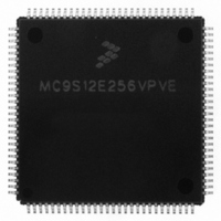
MC9S12E256VPVE Freescale Semiconductor, MC9S12E256VPVE Datasheet - Page 551

MC9S12E256VPVE
Manufacturer Part Number
MC9S12E256VPVE
Description
IC MCU 256K FLASH 25MHZ 112-LQFP
Manufacturer
Freescale Semiconductor
Series
HCS12r
Datasheet
1.MC9S12E256CFUE.pdf
(602 pages)
Specifications of MC9S12E256VPVE
Core Processor
HCS12
Core Size
16-Bit
Speed
25MHz
Connectivity
EBI/EMI, I²C, SCI, SPI
Peripherals
POR, PWM, WDT
Number Of I /o
91
Program Memory Size
256KB (256K x 8)
Program Memory Type
FLASH
Ram Size
16K x 8
Voltage - Supply (vcc/vdd)
2.35 V ~ 2.75 V
Data Converters
A/D 16x10b; D/A 2x8b
Oscillator Type
Internal
Operating Temperature
-40°C ~ 105°C
Package / Case
112-LQFP
Processor Series
S12E
Core
HCS12
Data Bus Width
16 bit
Data Ram Size
16 KB
Interface Type
I2C/SCI/SPI
Maximum Clock Frequency
50 MHz
Number Of Programmable I/os
92
Number Of Timers
12
Maximum Operating Temperature
+ 105 C
Mounting Style
SMD/SMT
3rd Party Development Tools
EWHCS12
Minimum Operating Temperature
- 40 C
On-chip Adc
16-ch x 10-bit
On-chip Dac
2-ch x 8-bit
For Use With
M68EVB912E128 - BOARD EVAL FOR MC9S12E128/64
Lead Free Status / RoHS Status
Lead free / RoHS Compliant
Eeprom Size
-
Lead Free Status / Rohs Status
Lead free / RoHS Compliant
Available stocks
Company
Part Number
Manufacturer
Quantity
Price
Company:
Part Number:
MC9S12E256VPVE
Manufacturer:
Freescale Semiconductor
Quantity:
10 000
- Current page: 551 of 602
- Download datasheet (4Mb)
19.3.2.9
Read: Anytime
Write: Determined at chip integration. Generally it’s: “write anytime in all modes;” on some devices it will
be: “write only in special modes.” Check specific device documentation to determine which applies.
Reset: Defined at chip integration as either 0x00 (paired with write in any mode) or 0x3C (paired with
write only in special modes), see
Freescale Semiconductor
1. The reset state of this register is controlled at chip integration. Please refer to
Reset
(MC9S12E256DGV1)”
W
R
1
Program Page Index Register (PPAGE)
—
0
7
As stated, the bits in this register provide read visibility to the system
memory space and on-chip/off-chip partitioning allocations defined at
system integration. The actual array size for any given type of memory
block may differ from the allocated size. Please refer to
“MC9S12E256 Device Overview (MC9S12E256DGV1)”
NOTES:
1. The ROMHM software bit in the MISC register determines the accessibility of the
FLASH/ROM memory space. Please refer to
1
(MEMSIZ1),” for a detailed functional description of the ROMHM bit.
pag_sw1:pag_sw0
= Unimplemented or Reserved
to determine the actual reset state of this register.
Table 19-11. Allocated FLASH/ROM Physical Memory Space
rom_sw1:rom_sw0
—
0
6
00
01
10
11
Figure 19-11. Program Page Index Register (PPAGE)
Table 19-12. Allocated Off-Chip Memory Options
00
01
10
11
Chapter 1, “MC9S12E256 Device Overview
PIX5
MC9S12E256 Data Sheet, Rev. 1.08
—
5
Off-Chip Space
876K bytes
768K bytes
512K bytes
PIX4
NOTE
0K byte
—
4
Section 19.3.2.8, “Memory Size Register
PIX3
—
3
Allocated FLASH
or ROM Space
48K bytes
64K bytes
Chapter 1, “MC9S12E256 Device Overview
16K bytes
0K byte
Chapter 19 Module Mapping Control (MMCV4)
On-Chip Space
Chapter 1,
PIX2
128K bytes
256K bytes
512K bytes
for actual sizes.
—
1M byte
2
(1)
(1)
(MC9S12E256DGV1)”.
PIX1
—
1
PIX0
—
0
551
Related parts for MC9S12E256VPVE
Image
Part Number
Description
Manufacturer
Datasheet
Request
R
Part Number:
Description:
Manufacturer:
Freescale Semiconductor, Inc
Datasheet:
Part Number:
Description:
Manufacturer:
Freescale Semiconductor, Inc
Datasheet:
Part Number:
Description:
Manufacturer:
Freescale Semiconductor, Inc
Datasheet:
Part Number:
Description:
Manufacturer:
Freescale Semiconductor, Inc
Datasheet:
Part Number:
Description:
Manufacturer:
Freescale Semiconductor, Inc
Datasheet:
Part Number:
Description:
Manufacturer:
Freescale Semiconductor, Inc
Datasheet:
Part Number:
Description:
Manufacturer:
Freescale Semiconductor, Inc
Datasheet:
Part Number:
Description:
Manufacturer:
Freescale Semiconductor, Inc
Datasheet:
Part Number:
Description:
Manufacturer:
Freescale Semiconductor, Inc
Datasheet:
Part Number:
Description:
Manufacturer:
Freescale Semiconductor, Inc
Datasheet:
Part Number:
Description:
Manufacturer:
Freescale Semiconductor, Inc
Datasheet:
Part Number:
Description:
Manufacturer:
Freescale Semiconductor, Inc
Datasheet:
Part Number:
Description:
Manufacturer:
Freescale Semiconductor, Inc
Datasheet:
Part Number:
Description:
Manufacturer:
Freescale Semiconductor, Inc
Datasheet:
Part Number:
Description:
Manufacturer:
Freescale Semiconductor, Inc
Datasheet:


