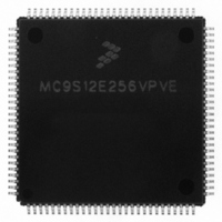
MC9S12E256VPVE Freescale Semiconductor, MC9S12E256VPVE Datasheet - Page 130

MC9S12E256VPVE
Manufacturer Part Number
MC9S12E256VPVE
Description
IC MCU 256K FLASH 25MHZ 112-LQFP
Manufacturer
Freescale Semiconductor
Series
HCS12r
Datasheet
1.MC9S12E256CFUE.pdf
(602 pages)
Specifications of MC9S12E256VPVE
Core Processor
HCS12
Core Size
16-Bit
Speed
25MHz
Connectivity
EBI/EMI, I²C, SCI, SPI
Peripherals
POR, PWM, WDT
Number Of I /o
91
Program Memory Size
256KB (256K x 8)
Program Memory Type
FLASH
Ram Size
16K x 8
Voltage - Supply (vcc/vdd)
2.35 V ~ 2.75 V
Data Converters
A/D 16x10b; D/A 2x8b
Oscillator Type
Internal
Operating Temperature
-40°C ~ 105°C
Package / Case
112-LQFP
Processor Series
S12E
Core
HCS12
Data Bus Width
16 bit
Data Ram Size
16 KB
Interface Type
I2C/SCI/SPI
Maximum Clock Frequency
50 MHz
Number Of Programmable I/os
92
Number Of Timers
12
Maximum Operating Temperature
+ 105 C
Mounting Style
SMD/SMT
3rd Party Development Tools
EWHCS12
Minimum Operating Temperature
- 40 C
On-chip Adc
16-ch x 10-bit
On-chip Dac
2-ch x 8-bit
For Use With
M68EVB912E128 - BOARD EVAL FOR MC9S12E128/64
Lead Free Status / RoHS Status
Lead free / RoHS Compliant
Eeprom Size
-
Lead Free Status / Rohs Status
Lead free / RoHS Compliant
Available stocks
Company
Part Number
Manufacturer
Quantity
Price
Company:
Part Number:
MC9S12E256VPVE
Manufacturer:
Freescale Semiconductor
Quantity:
10 000
- Current page: 130 of 602
- Download datasheet (4Mb)
Chapter 3 Port Integration Module (PIM9E256V1)
3.3.1
Port AD is associated with the analog-to-digital converter (ATD) and keyboard wake-up (KWU)
interrupts. Each pin is assigned to these modules according to the following priority: ATD > KWU >
general-purpose I/O.
For the pins of port AD to be used as inputs, the corresponding bits of the ATDDIEN0 and ATDDIEN1
registers in the ATD module must be set to 1 (digital input buffer is enabled). The ATDDIEN0 and
ATDDIEN1 registers do not affect the port AD pins when they are configured as outputs.
Refer to
and ATDDIEN1 registers.
During reset, port AD pins are configured as high-impedance analog inputs (digital input buffer is
disabled).
3.3.1.1
Read: Anytime. Write: Anytime.
If the data direction bit of the associated I/O pin (DDRADx) is set to 1 (output), a write to the
corresponding I/O Register bit sets the value to be driven to the Port AD pin. If the data direction bit of the
associated I/O pin (DDRADx) is set to 0 (input), a write to the corresponding I/O Register bit takes place
but has no effect on the Port AD pin.
If the associated data direction bit (DDRADx) is set to 1 (output), a read returns the value of the I/O register
bit.
If the associated data direction bit (DDRADx) is set to 0 (input) and the associated ATDDIEN0(1) bit is
set to 0 (digital input buffer is disabled), the associated I/O register bit (PTADx) reads “1”.
If the associated data direction bit (DDRADx) is set to 0 (input) and the associated ATDDIEN0(1) bit is
set to 1 (digital input buffer is enabled), a read returns the value of the pin.
130
KWU:
Reset
KWU:
Reset
ATD:
ATD:
W
W
R
R
Chapter 6, “Analog-to-Digital Converter (ATD10B16CV4)”
KWAD15
PTAD15
KWAD7
PTAD7
Port AD
AN15
AN7
Port AD I/O Register (PTAD)
0
0
7
7
KWAD14
PTAD14
KWAD6
PTAD6
AN14
AN6
0
0
6
6
Figure 3-2. Port AD I/O Register (PTAD)
KWAD13
PTAD13
KWAD5
PTAD5
AN13
AN5
MC9S12E256 Data Sheet, Rev. 1.08
0
0
5
5
PTAD12
KWAD4
KWA12
PTAD4
AN12
AN4
0
0
4
4
KWAD11
PTAD11
KWAD3
PTAD3
AN11
AN3
3
0
3
0
for information on the ATDDIEN0
KWAD10
PTAD10
KWAD2
PTAD2
AN10
AN2
0
0
2
2
KWAD9
KWAD1
PTAD9
PTAD1
Freescale Semiconductor
AN9
AN1
1
0
1
0
KWAD8
KWAD0
PTAD8
PTAD0
AN8
AN0
0
0
0
0
Related parts for MC9S12E256VPVE
Image
Part Number
Description
Manufacturer
Datasheet
Request
R
Part Number:
Description:
Manufacturer:
Freescale Semiconductor, Inc
Datasheet:
Part Number:
Description:
Manufacturer:
Freescale Semiconductor, Inc
Datasheet:
Part Number:
Description:
Manufacturer:
Freescale Semiconductor, Inc
Datasheet:
Part Number:
Description:
Manufacturer:
Freescale Semiconductor, Inc
Datasheet:
Part Number:
Description:
Manufacturer:
Freescale Semiconductor, Inc
Datasheet:
Part Number:
Description:
Manufacturer:
Freescale Semiconductor, Inc
Datasheet:
Part Number:
Description:
Manufacturer:
Freescale Semiconductor, Inc
Datasheet:
Part Number:
Description:
Manufacturer:
Freescale Semiconductor, Inc
Datasheet:
Part Number:
Description:
Manufacturer:
Freescale Semiconductor, Inc
Datasheet:
Part Number:
Description:
Manufacturer:
Freescale Semiconductor, Inc
Datasheet:
Part Number:
Description:
Manufacturer:
Freescale Semiconductor, Inc
Datasheet:
Part Number:
Description:
Manufacturer:
Freescale Semiconductor, Inc
Datasheet:
Part Number:
Description:
Manufacturer:
Freescale Semiconductor, Inc
Datasheet:
Part Number:
Description:
Manufacturer:
Freescale Semiconductor, Inc
Datasheet:
Part Number:
Description:
Manufacturer:
Freescale Semiconductor, Inc
Datasheet:


