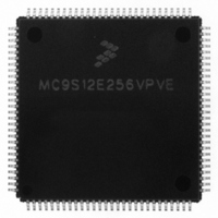
MC9S12E256VPVE Freescale Semiconductor, MC9S12E256VPVE Datasheet - Page 263

MC9S12E256VPVE
Manufacturer Part Number
MC9S12E256VPVE
Description
IC MCU 256K FLASH 25MHZ 112-LQFP
Manufacturer
Freescale Semiconductor
Series
HCS12r
Datasheet
1.MC9S12E256CFUE.pdf
(602 pages)
Specifications of MC9S12E256VPVE
Core Processor
HCS12
Core Size
16-Bit
Speed
25MHz
Connectivity
EBI/EMI, I²C, SCI, SPI
Peripherals
POR, PWM, WDT
Number Of I /o
91
Program Memory Size
256KB (256K x 8)
Program Memory Type
FLASH
Ram Size
16K x 8
Voltage - Supply (vcc/vdd)
2.35 V ~ 2.75 V
Data Converters
A/D 16x10b; D/A 2x8b
Oscillator Type
Internal
Operating Temperature
-40°C ~ 105°C
Package / Case
112-LQFP
Processor Series
S12E
Core
HCS12
Data Bus Width
16 bit
Data Ram Size
16 KB
Interface Type
I2C/SCI/SPI
Maximum Clock Frequency
50 MHz
Number Of Programmable I/os
92
Number Of Timers
12
Maximum Operating Temperature
+ 105 C
Mounting Style
SMD/SMT
3rd Party Development Tools
EWHCS12
Minimum Operating Temperature
- 40 C
On-chip Adc
16-ch x 10-bit
On-chip Dac
2-ch x 8-bit
For Use With
M68EVB912E128 - BOARD EVAL FOR MC9S12E128/64
Lead Free Status / RoHS Status
Lead free / RoHS Compliant
Eeprom Size
-
Lead Free Status / Rohs Status
Lead free / RoHS Compliant
Available stocks
Company
Part Number
Manufacturer
Quantity
Price
Company:
Part Number:
MC9S12E256VPVE
Manufacturer:
Freescale Semiconductor
Quantity:
10 000
- Current page: 263 of 602
- Download datasheet (4Mb)
8.4.5
8.4.5.1
The SCI receiver can accommodate either 8-bit or 9-bit data characters. The state of the M bit in SCI
control register 1 (SCICR1) determines the length of data characters. When receiving 9-bit data, bit R8 in
SCI data register high (SCIDRH) is the ninth bit (bit 8).
8.4.5.2
During an SCI reception, the receive shift register shifts a frame in from the RXD pin. The SCI data
register is the read-only buffer between the internal data bus and the receive shift register.
After a complete frame shifts into the receive shift register, the data portion of the frame transfers to the
SCI data register. The receive data register full flag, RDRF, in SCI status register 1 (SCISR1) becomes set,
Freescale Semiconductor
FROM TXD PIN
OR TRANSMITTER
SCRXD
LOOPS
Receiver
RSRC
RDRF/OR INTERRUPT REQUEST
Receiver Character Length
Character Reception
TDRE flag is set and immediately before writing the next byte to the SCI
data register.
If the TE bit is clear and the transmission is complete, the SCI is not the
master of the TXD pin
IDLE INTERRUPT REQUEST
RXPOL
CONTROL
LOOP
SBR12–SBR0
CLOCK
BUS
Figure 8-14. SCI Receiver Block Diagram
WAKE
DIVIDER
RAF
BAUD
ILT
RE
PE
PT
M
MC9S12E256 Data Sheet, Rev. 1.08
RECOVERY
DATA
CHECKING
WAKEUP
PARITY
LOGIC
INTERNAL BUS
IDLE
ILIE
RIE
H
Chapter 8 Serial Communication Interface (SCIV4)
11-BIT RECEIVE SHIFT REGISTER
8
7
SCI DATA REGISTER
RDRF
OR
6
5
R8
4
FE
NF
PE
3
2
1
0
L
RWU
263
Related parts for MC9S12E256VPVE
Image
Part Number
Description
Manufacturer
Datasheet
Request
R
Part Number:
Description:
Manufacturer:
Freescale Semiconductor, Inc
Datasheet:
Part Number:
Description:
Manufacturer:
Freescale Semiconductor, Inc
Datasheet:
Part Number:
Description:
Manufacturer:
Freescale Semiconductor, Inc
Datasheet:
Part Number:
Description:
Manufacturer:
Freescale Semiconductor, Inc
Datasheet:
Part Number:
Description:
Manufacturer:
Freescale Semiconductor, Inc
Datasheet:
Part Number:
Description:
Manufacturer:
Freescale Semiconductor, Inc
Datasheet:
Part Number:
Description:
Manufacturer:
Freescale Semiconductor, Inc
Datasheet:
Part Number:
Description:
Manufacturer:
Freescale Semiconductor, Inc
Datasheet:
Part Number:
Description:
Manufacturer:
Freescale Semiconductor, Inc
Datasheet:
Part Number:
Description:
Manufacturer:
Freescale Semiconductor, Inc
Datasheet:
Part Number:
Description:
Manufacturer:
Freescale Semiconductor, Inc
Datasheet:
Part Number:
Description:
Manufacturer:
Freescale Semiconductor, Inc
Datasheet:
Part Number:
Description:
Manufacturer:
Freescale Semiconductor, Inc
Datasheet:
Part Number:
Description:
Manufacturer:
Freescale Semiconductor, Inc
Datasheet:
Part Number:
Description:
Manufacturer:
Freescale Semiconductor, Inc
Datasheet:


