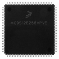
MC9S12E256VPVE Freescale Semiconductor, MC9S12E256VPVE Datasheet - Page 592

MC9S12E256VPVE
Manufacturer Part Number
MC9S12E256VPVE
Description
IC MCU 256K FLASH 25MHZ 112-LQFP
Manufacturer
Freescale Semiconductor
Series
HCS12r
Datasheet
1.MC9S12E256CFUE.pdf
(602 pages)
Specifications of MC9S12E256VPVE
Core Processor
HCS12
Core Size
16-Bit
Speed
25MHz
Connectivity
EBI/EMI, I²C, SCI, SPI
Peripherals
POR, PWM, WDT
Number Of I /o
91
Program Memory Size
256KB (256K x 8)
Program Memory Type
FLASH
Ram Size
16K x 8
Voltage - Supply (vcc/vdd)
2.35 V ~ 2.75 V
Data Converters
A/D 16x10b; D/A 2x8b
Oscillator Type
Internal
Operating Temperature
-40°C ~ 105°C
Package / Case
112-LQFP
Processor Series
S12E
Core
HCS12
Data Bus Width
16 bit
Data Ram Size
16 KB
Interface Type
I2C/SCI/SPI
Maximum Clock Frequency
50 MHz
Number Of Programmable I/os
92
Number Of Timers
12
Maximum Operating Temperature
+ 105 C
Mounting Style
SMD/SMT
3rd Party Development Tools
EWHCS12
Minimum Operating Temperature
- 40 C
On-chip Adc
16-ch x 10-bit
On-chip Dac
2-ch x 8-bit
For Use With
M68EVB912E128 - BOARD EVAL FOR MC9S12E128/64
Lead Free Status / RoHS Status
Lead free / RoHS Compliant
Eeprom Size
-
Lead Free Status / Rohs Status
Lead free / RoHS Compliant
Available stocks
Company
Part Number
Manufacturer
Quantity
Price
Company:
Part Number:
MC9S12E256VPVE
Manufacturer:
Freescale Semiconductor
Quantity:
10 000
- Current page: 592 of 602
- Download datasheet (4Mb)
Appendix A Electrical Characteristics
1
592
Conditions are 4.75V < VDDX < 5.25V, Junction Temperature -40°C to +140°C, C
Num
Affected by clock stretch: add N x t
10
11
12
13
14
15
16
17
18
19
20
21
22
23
24
25
26
27
28
29
30
31
32
33
34
35
36
1
2
3
4
5
6
7
8
9
C
P
P
D
D
D
D
D
D
D
D
D
D
D
D
D
D
D
D
D
D
D
D
D
D
D
D
D
D
D
D
D
D
D
D
D
D
Frequency of operation (E-clock)
Cycle time
Pulse width, E low
Pulse width, E high
Address delay time
Address valid time to E rise (PW
Muxed address hold time
Address hold to data valid
Data hold to address
Read data setup time
Read data hold time
Write data delay time
Write data hold time
Write data setup time
Address access time
E high access time
Non-multiplexed address delay time
Non-muxed address valid to E rise (PW
Non-multiplexed address hold time
Chip select delay time
Chip select access time
Chip select hold time
Chip select negated time
Read/write delay time
Read/write valid time to E rise (PW
Read/write hold time
Low strobe delay time
Low strobe valid time to E rise (PW
Low strobe hold time
NOACC strobe delay time
NOACC valid time to E rise (PW
NOACC hold time
IPIPO[1:0] delay time
IPIPO[1:0] valid time to E rise (PW
IPIPO[1:0] delay time
IPIPO[1:0] valid time to E fall
Table A-26. Expanded Bus Timing Characteristics (5V Range)
cyc
1
1
(PW
1
Rating
1
1
where N=0,1,2 or 3, depending on the number of clock stretches.
(t
(PW
(PW
cyc
1
EH
(t
MC9S12E256 Data Sheet, Rev. 1.08
–t
cyc
EH
–t
EH
AD
DSR
–t
-t
–t
–t
P1V
CSD
DDW
EL
EL
DSR
)
–t
EL
)
–t
EL
EL
–t
)
NOD
AD
)
–t
DSR
–t
–t
P0D
)
RWD
LSD
EL
)
)
–t
)
)
)
NAD
)
Symbol
PW
PW
t
t
t
t
t
t
t
t
t
t
t
t
t
t
t
AHDS
t
t
ACCA
ACCE
t
t
t
t
ACCS
t
t
t
t
t
t
t
t
t
DDW
DHW
DSW
RWD
RWH
t
MAH
DHR
RWV
NOD
NOH
t
DHA
DSR
NAD
NAH
CSD
CSH
CSN
NOV
t
NAV
LSD
LSV
LSH
P0D
P0V
P1D
P1V
cyc
AD
f
AV
o
EH
EL
LOAD
Min
40
19
19
11
13
12
19
14
11
14
14
14
11
11
—
—
—
—
—
—
—
= 50pF
0
2
7
2
0
2
6
2
2
8
2
2
2
2
2
Typ
—
—
—
—
—
—
—
—
—
—
—
—
—
—
—
—
—
—
—
—
—
—
—
—
—
—
—
—
—
—
—
—
—
—
—
—
Freescale Semiconductor
Max
25.0
—
—
—
—
—
—
—
—
—
—
—
—
—
—
—
16
—
—
—
—
—
—
—
—
—
—
25
—
8
7
6
7
7
7
7
Unit
MHz
ns
ns
ns
ns
ns
ns
ns
ns
ns
ns
ns
ns
ns
ns
ns
ns
ns
ns
ns
ns
ns
ns
ns
ns
ns
ns
ns
ns
ns
ns
ns
ns
ns
ns
ns
Related parts for MC9S12E256VPVE
Image
Part Number
Description
Manufacturer
Datasheet
Request
R
Part Number:
Description:
Manufacturer:
Freescale Semiconductor, Inc
Datasheet:
Part Number:
Description:
Manufacturer:
Freescale Semiconductor, Inc
Datasheet:
Part Number:
Description:
Manufacturer:
Freescale Semiconductor, Inc
Datasheet:
Part Number:
Description:
Manufacturer:
Freescale Semiconductor, Inc
Datasheet:
Part Number:
Description:
Manufacturer:
Freescale Semiconductor, Inc
Datasheet:
Part Number:
Description:
Manufacturer:
Freescale Semiconductor, Inc
Datasheet:
Part Number:
Description:
Manufacturer:
Freescale Semiconductor, Inc
Datasheet:
Part Number:
Description:
Manufacturer:
Freescale Semiconductor, Inc
Datasheet:
Part Number:
Description:
Manufacturer:
Freescale Semiconductor, Inc
Datasheet:
Part Number:
Description:
Manufacturer:
Freescale Semiconductor, Inc
Datasheet:
Part Number:
Description:
Manufacturer:
Freescale Semiconductor, Inc
Datasheet:
Part Number:
Description:
Manufacturer:
Freescale Semiconductor, Inc
Datasheet:
Part Number:
Description:
Manufacturer:
Freescale Semiconductor, Inc
Datasheet:
Part Number:
Description:
Manufacturer:
Freescale Semiconductor, Inc
Datasheet:
Part Number:
Description:
Manufacturer:
Freescale Semiconductor, Inc
Datasheet:


