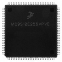
MC9S12E256VPVE Freescale Semiconductor, MC9S12E256VPVE Datasheet - Page 366

MC9S12E256VPVE
Manufacturer Part Number
MC9S12E256VPVE
Description
IC MCU 256K FLASH 25MHZ 112-LQFP
Manufacturer
Freescale Semiconductor
Series
HCS12r
Datasheet
1.MC9S12E256CFUE.pdf
(602 pages)
Specifications of MC9S12E256VPVE
Core Processor
HCS12
Core Size
16-Bit
Speed
25MHz
Connectivity
EBI/EMI, I²C, SCI, SPI
Peripherals
POR, PWM, WDT
Number Of I /o
91
Program Memory Size
256KB (256K x 8)
Program Memory Type
FLASH
Ram Size
16K x 8
Voltage - Supply (vcc/vdd)
2.35 V ~ 2.75 V
Data Converters
A/D 16x10b; D/A 2x8b
Oscillator Type
Internal
Operating Temperature
-40°C ~ 105°C
Package / Case
112-LQFP
Processor Series
S12E
Core
HCS12
Data Bus Width
16 bit
Data Ram Size
16 KB
Interface Type
I2C/SCI/SPI
Maximum Clock Frequency
50 MHz
Number Of Programmable I/os
92
Number Of Timers
12
Maximum Operating Temperature
+ 105 C
Mounting Style
SMD/SMT
3rd Party Development Tools
EWHCS12
Minimum Operating Temperature
- 40 C
On-chip Adc
16-ch x 10-bit
On-chip Dac
2-ch x 8-bit
For Use With
M68EVB912E128 - BOARD EVAL FOR MC9S12E128/64
Lead Free Status / RoHS Status
Lead free / RoHS Compliant
Eeprom Size
-
Lead Free Status / Rohs Status
Lead free / RoHS Compliant
Available stocks
Company
Part Number
Manufacturer
Quantity
Price
Company:
Part Number:
MC9S12E256VPVE
Manufacturer:
Freescale Semiconductor
Quantity:
10 000
- Current page: 366 of 602
- Download datasheet (4Mb)
Chapter 11 Pulse Width Modulator with Fault Protection (PMF15B6CV2)
11.4.6
Setting output control enable bit, OUTCTLx, enables software to drive the PWM outputs rather than the
PWM generator. In an independent mode, with OUTCTLx = 1, the output bit OUTx, controls the PWMx
channel. In a complementary channel operation the even OUTCTL bit is used to enable software output
control for the pair. But the OUTCTL bits must be switched in pairs for proper operation. The OUTCTLx
and OUTx bits are in the PWM output control register.
In independent PWM operation, setting or clearing the OUTx bit activates or deactivates the PWMx
output.
In complementary channel operation, the even-numbered OUTx bits replace the PWM generator outputs
as inputs to the deadtime generators. Complementary channel pairs still cannot be active simultaneously,
and the deadtime generators continue to insert deadtime in both channels of that pair, whenever an even
OUTx bit toggles. Even OUTx bits control the top PWM signals while the odd OUTx bits control the
bottom PWM signals with respect to the even OUTx bits. Setting the odd OUTx bit makes its
corresponding PWMx the complement of its even pair, while clearing the odd OUTx bit deactivates the
odd PWMx.
366
Software Output Control
NEGATIVE POLARITY
POSITIVE POLARITY
CENTER-ALIGNED
CENTER-ALIGNED
During software output control, TOPNEG and BOTNEG still control output
polarity. It will take upto 3 clock cycles to see the effect of output control on
the PWM output pins.
UP/DOWN COUNTER
UP/DOWN COUNTER
MODULUS = 4
MODULUS = 4
PWM = 0
PWM = 1
PWM = 2
PWM = 3
PWM = 4
PWM = 0
PWM = 1
PWM = 2
PWM = 3
PWM = 4
MC9S12E256 Data Sheet, Rev. 1.08
Figure 11-61. PWM Polarity
NOTE
NEGATIVE POLARITY
POSITIVE POLARITY
EDGE-ALIGNED
EDGE-ALIGNED
MODULUS = 4
UP COUNTER
MODULUS = 4
UP COUNTER
PWM = 0
PWM = 1
PWM = 2
PWM = 3
PWM = 4
PWM = 0
PWM = 1
PWM = 2
PWM = 3
PWM = 4
Freescale Semiconductor
Related parts for MC9S12E256VPVE
Image
Part Number
Description
Manufacturer
Datasheet
Request
R
Part Number:
Description:
Manufacturer:
Freescale Semiconductor, Inc
Datasheet:
Part Number:
Description:
Manufacturer:
Freescale Semiconductor, Inc
Datasheet:
Part Number:
Description:
Manufacturer:
Freescale Semiconductor, Inc
Datasheet:
Part Number:
Description:
Manufacturer:
Freescale Semiconductor, Inc
Datasheet:
Part Number:
Description:
Manufacturer:
Freescale Semiconductor, Inc
Datasheet:
Part Number:
Description:
Manufacturer:
Freescale Semiconductor, Inc
Datasheet:
Part Number:
Description:
Manufacturer:
Freescale Semiconductor, Inc
Datasheet:
Part Number:
Description:
Manufacturer:
Freescale Semiconductor, Inc
Datasheet:
Part Number:
Description:
Manufacturer:
Freescale Semiconductor, Inc
Datasheet:
Part Number:
Description:
Manufacturer:
Freescale Semiconductor, Inc
Datasheet:
Part Number:
Description:
Manufacturer:
Freescale Semiconductor, Inc
Datasheet:
Part Number:
Description:
Manufacturer:
Freescale Semiconductor, Inc
Datasheet:
Part Number:
Description:
Manufacturer:
Freescale Semiconductor, Inc
Datasheet:
Part Number:
Description:
Manufacturer:
Freescale Semiconductor, Inc
Datasheet:
Part Number:
Description:
Manufacturer:
Freescale Semiconductor, Inc
Datasheet:


