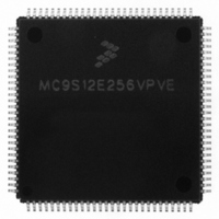
MC9S12E256VPVE Freescale Semiconductor, MC9S12E256VPVE Datasheet - Page 439

MC9S12E256VPVE
Manufacturer Part Number
MC9S12E256VPVE
Description
IC MCU 256K FLASH 25MHZ 112-LQFP
Manufacturer
Freescale Semiconductor
Series
HCS12r
Datasheet
1.MC9S12E256CFUE.pdf
(602 pages)
Specifications of MC9S12E256VPVE
Core Processor
HCS12
Core Size
16-Bit
Speed
25MHz
Connectivity
EBI/EMI, I²C, SCI, SPI
Peripherals
POR, PWM, WDT
Number Of I /o
91
Program Memory Size
256KB (256K x 8)
Program Memory Type
FLASH
Ram Size
16K x 8
Voltage - Supply (vcc/vdd)
2.35 V ~ 2.75 V
Data Converters
A/D 16x10b; D/A 2x8b
Oscillator Type
Internal
Operating Temperature
-40°C ~ 105°C
Package / Case
112-LQFP
Processor Series
S12E
Core
HCS12
Data Bus Width
16 bit
Data Ram Size
16 KB
Interface Type
I2C/SCI/SPI
Maximum Clock Frequency
50 MHz
Number Of Programmable I/os
92
Number Of Timers
12
Maximum Operating Temperature
+ 105 C
Mounting Style
SMD/SMT
3rd Party Development Tools
EWHCS12
Minimum Operating Temperature
- 40 C
On-chip Adc
16-ch x 10-bit
On-chip Dac
2-ch x 8-bit
For Use With
M68EVB912E128 - BOARD EVAL FOR MC9S12E128/64
Lead Free Status / RoHS Status
Lead free / RoHS Compliant
Eeprom Size
-
Lead Free Status / Rohs Status
Lead free / RoHS Compliant
Available stocks
Company
Part Number
Manufacturer
Quantity
Price
Company:
Part Number:
MC9S12E256VPVE
Manufacturer:
Freescale Semiconductor
Quantity:
10 000
- Current page: 439 of 602
- Download datasheet (4Mb)
14.2
Due to the nature of VREG being a voltage regulator providing the chip internal power supply voltages
most signals are power supply signals connected to pads.
Table 14-1
14.2.1
Signal V
pin. A chip external decoupling capacitor (100 nF...220 nF, X7R ceramic) between V
smoothen ripple on V
For entering shutdown mode, pin V
14.2.2
Signals V
regulator. Internal precision reference circuits are supplied from these signals. A chip external decoupling
capacitor (100 nF...220 nF, X7R ceramic) between V
supply.
Freescale Semiconductor
V
REGEN
V
V
Name
DDR
V
V
V
DDPLL
V
SSPLL
External Signal Description
V
DDA
DDR
DDA
SSA
DD
SS
(optional)
shows all signals of VREG associated with pins.
V
V
is the power input of VREG. All currents sourced into the regulator loads flow through this
DDR
DDA
/V
Check
(MC9S12E256DGV1)”
SSA
, V
— Regulator Power Input
which are supposed to be relatively quiet are used to supply the analog parts of the
DDR
Chapter 1, “MC9S12E256 Device Overview
SSA
Port
.
—
—
—
—
—
—
—
—
— Regulator Reference Supply
VREG power input (positive supply)
VREG quiet input (positive supply)
VREG quiet input (ground)
VREG primary output (positive supply)
VREG primary output (ground)
VREG secondary output (positive supply)
VREG secondary output (ground)
VREG (Optional) Regulator Enable
Table 14-1. VREG — Signal Properties
DDR
MC9S12E256 Data Sheet, Rev. 1.08
for connectivity of the signals.
should also be tied to ground on devices without a V
NOTE
Function
DDA
and V
Chapter 14 Dual Output Voltage Regulator (VREG3V3V2)
SSA
can further improve the quality of this
Reset State
DDR
—
—
—
—
—
—
—
—
and V
REGEN
SSR
Pull Up
—
—
—
—
—
—
—
—
can
pin.
439
Related parts for MC9S12E256VPVE
Image
Part Number
Description
Manufacturer
Datasheet
Request
R
Part Number:
Description:
Manufacturer:
Freescale Semiconductor, Inc
Datasheet:
Part Number:
Description:
Manufacturer:
Freescale Semiconductor, Inc
Datasheet:
Part Number:
Description:
Manufacturer:
Freescale Semiconductor, Inc
Datasheet:
Part Number:
Description:
Manufacturer:
Freescale Semiconductor, Inc
Datasheet:
Part Number:
Description:
Manufacturer:
Freescale Semiconductor, Inc
Datasheet:
Part Number:
Description:
Manufacturer:
Freescale Semiconductor, Inc
Datasheet:
Part Number:
Description:
Manufacturer:
Freescale Semiconductor, Inc
Datasheet:
Part Number:
Description:
Manufacturer:
Freescale Semiconductor, Inc
Datasheet:
Part Number:
Description:
Manufacturer:
Freescale Semiconductor, Inc
Datasheet:
Part Number:
Description:
Manufacturer:
Freescale Semiconductor, Inc
Datasheet:
Part Number:
Description:
Manufacturer:
Freescale Semiconductor, Inc
Datasheet:
Part Number:
Description:
Manufacturer:
Freescale Semiconductor, Inc
Datasheet:
Part Number:
Description:
Manufacturer:
Freescale Semiconductor, Inc
Datasheet:
Part Number:
Description:
Manufacturer:
Freescale Semiconductor, Inc
Datasheet:
Part Number:
Description:
Manufacturer:
Freescale Semiconductor, Inc
Datasheet:


