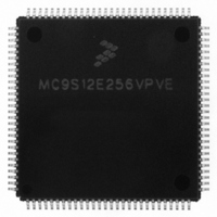
MC9S12E256VPVE Freescale Semiconductor, MC9S12E256VPVE Datasheet - Page 60

MC9S12E256VPVE
Manufacturer Part Number
MC9S12E256VPVE
Description
IC MCU 256K FLASH 25MHZ 112-LQFP
Manufacturer
Freescale Semiconductor
Series
HCS12r
Datasheet
1.MC9S12E256CFUE.pdf
(602 pages)
Specifications of MC9S12E256VPVE
Core Processor
HCS12
Core Size
16-Bit
Speed
25MHz
Connectivity
EBI/EMI, I²C, SCI, SPI
Peripherals
POR, PWM, WDT
Number Of I /o
91
Program Memory Size
256KB (256K x 8)
Program Memory Type
FLASH
Ram Size
16K x 8
Voltage - Supply (vcc/vdd)
2.35 V ~ 2.75 V
Data Converters
A/D 16x10b; D/A 2x8b
Oscillator Type
Internal
Operating Temperature
-40°C ~ 105°C
Package / Case
112-LQFP
Processor Series
S12E
Core
HCS12
Data Bus Width
16 bit
Data Ram Size
16 KB
Interface Type
I2C/SCI/SPI
Maximum Clock Frequency
50 MHz
Number Of Programmable I/os
92
Number Of Timers
12
Maximum Operating Temperature
+ 105 C
Mounting Style
SMD/SMT
3rd Party Development Tools
EWHCS12
Minimum Operating Temperature
- 40 C
On-chip Adc
16-ch x 10-bit
On-chip Dac
2-ch x 8-bit
For Use With
M68EVB912E128 - BOARD EVAL FOR MC9S12E128/64
Lead Free Status / RoHS Status
Lead free / RoHS Compliant
Eeprom Size
-
Lead Free Status / Rohs Status
Lead free / RoHS Compliant
Available stocks
Company
Part Number
Manufacturer
Quantity
Price
Company:
Part Number:
MC9S12E256VPVE
Manufacturer:
Freescale Semiconductor
Quantity:
10 000
- Current page: 60 of 602
- Download datasheet (4Mb)
Chapter 1 MC9S12E256 Device Overview (MC9S12E256DGV1)
1
If the port pins are not bonded out in the chosen package the user should initialize the registers to be inputs
with enabled pull resistance to avoid excess current consumption. This applies to the following pins:
60
Function 1
Pin Name
The Port E output buffer enable signal control at reset is determined by the PEAR register and is mode dependent. For
example, in special test mode RDWE = LSTRE = 1 which enables the PE[3:2] output buffers and disables the pull-ups. Refer
to
PQ[6:4]
PQ[3:0]
PU[7:6]
PU[5:4]
PP[5:0]
PU[3:0]
PT[7:4]
PT[3:0]
PM0
PS7
PS6
PS5
PS4
PS3
PS2
PS1
PS0
Chapter 18, “Multiplexed External Bus Interface (MEBIV3)”
(80QFP): Port A[7:0], Port B[7:0], Port E[6,5,3,2], Port K[7:0], Port U[7:4]
(64QFN): Port U[3:0], Port Q[6:4], Port M[3], Port AD[14,11,10,9,7,5,3,1]
Function 2
FAULT[3:0]
Pin Name
IOC1[7:4]
IOC0[7:4]
PW1[5:4]
IOC2[7:4]
PW0[5:0]
Signals shown in bold are not available in the 112-pin package.
Signals shown in italic are not available in the 80-pin package.
IS[6:4]
DAO0
RXD1
RXD0
MOSI
MISO
TXD1
TXD0
SCK
SS
—
Function 3
Pin Name
PW1[3:0]
—
—
—
—
—
—
—
—
—
—
—
—
—
—
—
—
MC9S12E256 Data Sheet, Rev. 1.08
Domain
Table 1-4. Signal Properties
Power
VDDX
VDDX
VDDX
VDDX
VDDX
VDDX
VDDX
VDDX
VDDX
VDDX
VDDX
VDDX
VDDX
VDDX
VDDX
VDDX
VDDX
PERM/
PERQ/
PERQ/
PERP/
PERS/
PERS/
PERS/
PERS/
PERS/
PERS/
PERS/
PERS/
PERT/
PERT/
PERU/
PERU/
PERU/
PPSM
CTRL
PPSP
PPSQ
PPSQ
PPSS
PPSS
PPSS
PPSS
PPSS
PPSS
PPSS
PPSS
PPSU
PPSU
PPSU
Internal Pull Resistor
PPST
PPST
NOTE
for PEAR register details.
Reset State
Disabled
Disabled
Disabled
Disabled
Disabled
Disabled
Disabled
Disabled
Disabled
Up
Up
Up
Up
Up
Up
Up
Up
Port M I/O Pin, DAC0 output
Port P I/O Pins, PWM output
Port Q I/O Pins, IS[6:4] input
Port Q I/O Pins, Fault[3:0] input
Port S I/O Pin, SPI SS signal
Port S I/O Pin, SPI SCK signal
Port S I/O Pin, SPI MOSI signal
Port S I/O Pin, SPI MISO signal
Port S I/O Pin, SCI1 transmit signal
Port S I/O Pin, SCI1 receive signal
Port S I/O Pin, SCI0 transmit signal
Port S I/O Pin, SCI0 receive signal
Port T I/O Pins, timer (TIM1)
Port T I/O Pins, timer (TIM0)
Port U I/O Pins
Port U I/O Pins, PWM outputs
Port U I/O Pins, timer (TIM2), PWM
outputs
Description
Freescale Semiconductor
Related parts for MC9S12E256VPVE
Image
Part Number
Description
Manufacturer
Datasheet
Request
R
Part Number:
Description:
Manufacturer:
Freescale Semiconductor, Inc
Datasheet:
Part Number:
Description:
Manufacturer:
Freescale Semiconductor, Inc
Datasheet:
Part Number:
Description:
Manufacturer:
Freescale Semiconductor, Inc
Datasheet:
Part Number:
Description:
Manufacturer:
Freescale Semiconductor, Inc
Datasheet:
Part Number:
Description:
Manufacturer:
Freescale Semiconductor, Inc
Datasheet:
Part Number:
Description:
Manufacturer:
Freescale Semiconductor, Inc
Datasheet:
Part Number:
Description:
Manufacturer:
Freescale Semiconductor, Inc
Datasheet:
Part Number:
Description:
Manufacturer:
Freescale Semiconductor, Inc
Datasheet:
Part Number:
Description:
Manufacturer:
Freescale Semiconductor, Inc
Datasheet:
Part Number:
Description:
Manufacturer:
Freescale Semiconductor, Inc
Datasheet:
Part Number:
Description:
Manufacturer:
Freescale Semiconductor, Inc
Datasheet:
Part Number:
Description:
Manufacturer:
Freescale Semiconductor, Inc
Datasheet:
Part Number:
Description:
Manufacturer:
Freescale Semiconductor, Inc
Datasheet:
Part Number:
Description:
Manufacturer:
Freescale Semiconductor, Inc
Datasheet:
Part Number:
Description:
Manufacturer:
Freescale Semiconductor, Inc
Datasheet:


