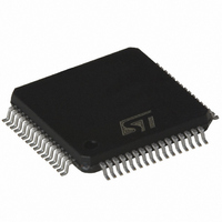
ST7FMC2R6T6 STMicroelectronics, ST7FMC2R6T6 Datasheet - Page 122

ST7FMC2R6T6
Manufacturer Part Number
ST7FMC2R6T6
Description
MCU 8BIT 32K FLASH 64TQFP
Manufacturer
STMicroelectronics
Series
ST7r
Datasheet
1.ST7FMC2S4T6.pdf
(309 pages)
Specifications of ST7FMC2R6T6
Core Processor
ST7
Core Size
8-Bit
Speed
8MHz
Connectivity
LINSCI, SPI
Peripherals
LVD, Motor Control PWM, POR, PWM, WDT
Number Of I /o
44
Program Memory Size
32KB (32K x 8)
Program Memory Type
FLASH
Ram Size
1K x 8
Voltage - Supply (vcc/vdd)
3.8 V ~ 5.5 V
Data Converters
A/D 16x10b
Oscillator Type
Internal
Operating Temperature
-40°C ~ 85°C
Package / Case
64-TQFP, 64-VQFP
Processor Series
ST7FMC2x
Core
ST7
Data Bus Width
8 bit
Data Ram Size
1 KB
Interface Type
SCI, SPI
Maximum Clock Frequency
8 MHz
Number Of Programmable I/os
60
Number Of Timers
3
Maximum Operating Temperature
+ 85 C
Mounting Style
SMD/SMT
Development Tools By Supplier
ST7MC-KIT/BLDC, ST7MDT50-EMU3, STX-RLINK
Minimum Operating Temperature
- 40 C
On-chip Adc
10 bit, 16 Channel
For Use With
497-8402 - BOARD EVAL COMPLETE INVERTER497-8400 - KIT IGBT PWR MODULE CTRL ST7MC497-6408 - BOARD EVAL BLDC SENSORLESS MOTOR497-4734 - EVAL KIT 3KW POWER DRIVER BOARD497-4733 - EVAL KIT 1KW POWER DRIVER BOARD497-4732 - EVAL KIT 300W POWER DRIVER BOARD497-4731 - EVAL KIT PWR DRIVER CONTROL BRD
Lead Free Status / RoHS Status
Lead free / RoHS Compliant
Eeprom Size
-
Lead Free Status / Rohs Status
Details
Other names
497-4868
Available stocks
Company
Part Number
Manufacturer
Quantity
Price
Company:
Part Number:
ST7FMC2R6T6
Manufacturer:
STMicroelectronics
Quantity:
10 000
- Current page: 122 of 309
- Download datasheet (6Mb)
ST7MC1xx/ST7MC2xx
LINSCI™ SERIAL COMMUNICATION INTERFACE (LIN Mode)
10.5.9 LIN Mode - Functional Description.
The block diagram of the Serial Control Interface,
in LIN slave mode is shown in
It uses six registers:
– 3 control registers: SCICR1, SCICR2 and
– 2 status registers: the SCISR register and the
– A baud rate register: LPR mapped at the SCI-
The bits dedicated to LIN are located in the
SCICR3. Refer to the register descriptions in
tion
10.5.9.1 Entering LIN Mode
To use the LINSCI in LIN mode the following con-
figuration must be set in SCICR3 register:
– Clear the M bit to configure 8-bit word length.
– Set the LINE bit.
Master
To enter master mode the LSLV bit must be reset
In this case, setting the SBK bit will send 13 low
bits.
Then the baud rate can programmed using the
SCIBRR, SCIERPR and SCIETPR registers.
In LIN master mode, the Conventional and / or Ex-
tended Prescaler define the baud rate (as in stand-
ard SCI mode)
122/309
1
SCICR3
LHLR register mapped at the SCIERPR address
BRR address and an associated fraction register
LPFR mapped at the SCIETPR address
10.5.10for the definitions of each bit.
Figure
66.
Sec-
Slave
Set the LSLV bit in the SCICR3 register to enter
LIN slave mode. In this case, setting the SBK bit
will have no effect.
In LIN Slave mode the LIN baud rate generator is
selected instead of the Conventional or Extended
Prescaler. The LIN baud rate generator is com-
mon to the transmitter and the receiver.
Then the baud rate can be programmed using
LPR and LPRF registers.
Note: It is mandatory to set the LIN configuration
first before programming LPR and LPRF, because
the LIN configuration uses a different baud rate
generator from the standard one.
10.5.9.2 LIN Transmission
In LIN mode the same procedure as in SCI mode
has to be applied for a LIN transmission.
To transmit the LIN Header the proceed as fol-
lows:
– First set the SBK bit in the SCICR2 register to
– reset the SBK bit
– Load the LIN Synch Field (0x55) in the SCIDR
– Wait until the SCIDR is empty (TDRE bit set in
– Load the LIN message Identifier in the SCIDR
start transmitting a 13-bit LIN Synch Break
register to request Synch Field transmission
the SCISR register)
register to request Identifier transmission.
Related parts for ST7FMC2R6T6
Image
Part Number
Description
Manufacturer
Datasheet
Request
R

Part Number:
Description:
STMicroelectronics [RIPPLE-CARRY BINARY COUNTER/DIVIDERS]
Manufacturer:
STMicroelectronics
Datasheet:

Part Number:
Description:
STMicroelectronics [LIQUID-CRYSTAL DISPLAY DRIVERS]
Manufacturer:
STMicroelectronics
Datasheet:

Part Number:
Description:
BOARD EVAL FOR MEMS SENSORS
Manufacturer:
STMicroelectronics
Datasheet:

Part Number:
Description:
NPN TRANSISTOR POWER MODULE
Manufacturer:
STMicroelectronics
Datasheet:

Part Number:
Description:
TURBOSWITCH ULTRA-FAST HIGH VOLTAGE DIODE
Manufacturer:
STMicroelectronics
Datasheet:

Part Number:
Description:
Manufacturer:
STMicroelectronics
Datasheet:

Part Number:
Description:
DIODE / SCR MODULE
Manufacturer:
STMicroelectronics
Datasheet:

Part Number:
Description:
DIODE / SCR MODULE
Manufacturer:
STMicroelectronics
Datasheet:

Part Number:
Description:
Search -----> STE16N100
Manufacturer:
STMicroelectronics
Datasheet:

Part Number:
Description:
Search ---> STE53NA50
Manufacturer:
STMicroelectronics
Datasheet:

Part Number:
Description:
NPN Transistor Power Module
Manufacturer:
STMicroelectronics
Datasheet:

Part Number:
Description:
DIODE / SCR MODULE
Manufacturer:
STMicroelectronics
Datasheet:


