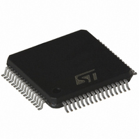
ST7FMC2R6T6 STMicroelectronics, ST7FMC2R6T6 Datasheet - Page 39

ST7FMC2R6T6
Manufacturer Part Number
ST7FMC2R6T6
Description
MCU 8BIT 32K FLASH 64TQFP
Manufacturer
STMicroelectronics
Series
ST7r
Datasheet
1.ST7FMC2S4T6.pdf
(309 pages)
Specifications of ST7FMC2R6T6
Core Processor
ST7
Core Size
8-Bit
Speed
8MHz
Connectivity
LINSCI, SPI
Peripherals
LVD, Motor Control PWM, POR, PWM, WDT
Number Of I /o
44
Program Memory Size
32KB (32K x 8)
Program Memory Type
FLASH
Ram Size
1K x 8
Voltage - Supply (vcc/vdd)
3.8 V ~ 5.5 V
Data Converters
A/D 16x10b
Oscillator Type
Internal
Operating Temperature
-40°C ~ 85°C
Package / Case
64-TQFP, 64-VQFP
Processor Series
ST7FMC2x
Core
ST7
Data Bus Width
8 bit
Data Ram Size
1 KB
Interface Type
SCI, SPI
Maximum Clock Frequency
8 MHz
Number Of Programmable I/os
60
Number Of Timers
3
Maximum Operating Temperature
+ 85 C
Mounting Style
SMD/SMT
Development Tools By Supplier
ST7MC-KIT/BLDC, ST7MDT50-EMU3, STX-RLINK
Minimum Operating Temperature
- 40 C
On-chip Adc
10 bit, 16 Channel
For Use With
497-8402 - BOARD EVAL COMPLETE INVERTER497-8400 - KIT IGBT PWR MODULE CTRL ST7MC497-6408 - BOARD EVAL BLDC SENSORLESS MOTOR497-4734 - EVAL KIT 3KW POWER DRIVER BOARD497-4733 - EVAL KIT 1KW POWER DRIVER BOARD497-4732 - EVAL KIT 300W POWER DRIVER BOARD497-4731 - EVAL KIT PWR DRIVER CONTROL BRD
Lead Free Status / RoHS Status
Lead free / RoHS Compliant
Eeprom Size
-
Lead Free Status / Rohs Status
Details
Other names
497-4868
Available stocks
Company
Part Number
Manufacturer
Quantity
Price
Company:
Part Number:
ST7FMC2R6T6
Manufacturer:
STMicroelectronics
Quantity:
10 000
- Current page: 39 of 309
- Download datasheet (6Mb)
MAIN CLOCK CONTROLLER WITH REAL-TIME CLOCK (Cont’d)
Bit 0 = OIF Oscillator interrupt flag
This bit is set by hardware and cleared by software
reading the CSR register. It indicates when set
that the main oscillator has reached the selected
elapsed time (TB1:0).
0: Timeout not reached
1: Timeout reached
CAUTION: The BRES and BSET instructions
must not be used on the MCCSR register to avoid
unintentionally clearing the OIF bit.
Table 5. Main Clock Controller Register Map and Reset Values
Address
002Dh
(Hex.)
002Ch
0040h
0040h
SICSR, page0
Reset Value
SICSR, page1
Reset Value
MCCSR
Reset Value
MCCBCR
Reset Value
Register
Label
PAGE
PAGE
MCO
7
0
0
0
0
VDIE
CP1
6
0
0
0
0
VCOEN
CP0
VDF
5
0
0
0
0
MCC BEEP CONTROL REGISTER (MCCBCR)
Read/Write
Reset Value: 0000 0000 (00h)
Bit 7:4 = Reserved, must be kept cleared.
Bit 3 = ADSTS A/D Converter Sample Time
Stretch
This bit is set and cleared by software to enable or
disable the A/D Converter sample time stretch fea-
ture.
0: AD sample time stretch disabled (for standard
1 AD sample time stretch enabled (for high imped-
Bit 2 = ADCIE A/D Converter Interrupt Enable
This bit is set and cleared by software to enable or
disable the A/D Converter interrupt.
0: AD Interrupt disabled
1 AD Interrupt enabled
Bit 1:0 = BC[1:0] Beep control
These 2 bits select the PF1 pin beep capability.
The beep output signal is available in Active-halt
mode but has to be disabled to reduce the con-
sumption.
impedance analog inputs)
ance analog inputs)
BC1
7
0
0
0
1
1
LVDRF
LOCK
SMS
4
x
x
0
0
0
BC0
0
1
0
1
ADSTS
PLLEN
TB1
0
3
0
0
0
0
Beep mode with f
0
~500-Hz
~1-KHz
~2-KHz
ADCIE
ST7MC1xx/ST7MC2xx
CFIE
TB0
2
0
0
0
0
STS
AD-
Off
ADC
CKSEL
IE
CSSD
BC1
~50% duty cycle
OIE
1
0
0
0
0
OSC2
Beep signal
BC1
Output
=8MHz
WDGRF
39/309
BC0
OIF
BC0
0
x
0
0
0
0
1
Related parts for ST7FMC2R6T6
Image
Part Number
Description
Manufacturer
Datasheet
Request
R

Part Number:
Description:
STMicroelectronics [RIPPLE-CARRY BINARY COUNTER/DIVIDERS]
Manufacturer:
STMicroelectronics
Datasheet:

Part Number:
Description:
STMicroelectronics [LIQUID-CRYSTAL DISPLAY DRIVERS]
Manufacturer:
STMicroelectronics
Datasheet:

Part Number:
Description:
BOARD EVAL FOR MEMS SENSORS
Manufacturer:
STMicroelectronics
Datasheet:

Part Number:
Description:
NPN TRANSISTOR POWER MODULE
Manufacturer:
STMicroelectronics
Datasheet:

Part Number:
Description:
TURBOSWITCH ULTRA-FAST HIGH VOLTAGE DIODE
Manufacturer:
STMicroelectronics
Datasheet:

Part Number:
Description:
Manufacturer:
STMicroelectronics
Datasheet:

Part Number:
Description:
DIODE / SCR MODULE
Manufacturer:
STMicroelectronics
Datasheet:

Part Number:
Description:
DIODE / SCR MODULE
Manufacturer:
STMicroelectronics
Datasheet:

Part Number:
Description:
Search -----> STE16N100
Manufacturer:
STMicroelectronics
Datasheet:

Part Number:
Description:
Search ---> STE53NA50
Manufacturer:
STMicroelectronics
Datasheet:

Part Number:
Description:
NPN Transistor Power Module
Manufacturer:
STMicroelectronics
Datasheet:

Part Number:
Description:
DIODE / SCR MODULE
Manufacturer:
STMicroelectronics
Datasheet:


