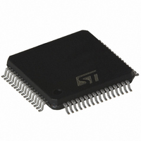
ST7FMC2R6T6 STMicroelectronics, ST7FMC2R6T6 Datasheet - Page 15

ST7FMC2R6T6
Manufacturer Part Number
ST7FMC2R6T6
Description
MCU 8BIT 32K FLASH 64TQFP
Manufacturer
STMicroelectronics
Series
ST7r
Datasheet
1.ST7FMC2S4T6.pdf
(309 pages)
Specifications of ST7FMC2R6T6
Core Processor
ST7
Core Size
8-Bit
Speed
8MHz
Connectivity
LINSCI, SPI
Peripherals
LVD, Motor Control PWM, POR, PWM, WDT
Number Of I /o
44
Program Memory Size
32KB (32K x 8)
Program Memory Type
FLASH
Ram Size
1K x 8
Voltage - Supply (vcc/vdd)
3.8 V ~ 5.5 V
Data Converters
A/D 16x10b
Oscillator Type
Internal
Operating Temperature
-40°C ~ 85°C
Package / Case
64-TQFP, 64-VQFP
Processor Series
ST7FMC2x
Core
ST7
Data Bus Width
8 bit
Data Ram Size
1 KB
Interface Type
SCI, SPI
Maximum Clock Frequency
8 MHz
Number Of Programmable I/os
60
Number Of Timers
3
Maximum Operating Temperature
+ 85 C
Mounting Style
SMD/SMT
Development Tools By Supplier
ST7MC-KIT/BLDC, ST7MDT50-EMU3, STX-RLINK
Minimum Operating Temperature
- 40 C
On-chip Adc
10 bit, 16 Channel
For Use With
497-8402 - BOARD EVAL COMPLETE INVERTER497-8400 - KIT IGBT PWR MODULE CTRL ST7MC497-6408 - BOARD EVAL BLDC SENSORLESS MOTOR497-4734 - EVAL KIT 3KW POWER DRIVER BOARD497-4733 - EVAL KIT 1KW POWER DRIVER BOARD497-4732 - EVAL KIT 300W POWER DRIVER BOARD497-4731 - EVAL KIT PWR DRIVER CONTROL BRD
Lead Free Status / RoHS Status
Lead free / RoHS Compliant
Eeprom Size
-
Lead Free Status / Rohs Status
Details
Other names
497-4868
Available stocks
Company
Part Number
Manufacturer
Quantity
Price
Company:
Part Number:
ST7FMC2R6T6
Manufacturer:
STMicroelectronics
Quantity:
10 000
- Current page: 15 of 309
- Download datasheet (6Mb)
Table 1. ST7MC Device Pin Description
Notes:
1. In the interrupt input column, “eiX” defines the associated external interrupt vector. If the weak pull-up
column (wpu) is merged with the interrupt column (int), then the I/O configuration is pull-up interrupt input,
else the configuration is floating interrupt input
2. If two alternate function outputs are enabled at the same time on a given pin (for instance, MCPWMV
and MCDEM on PD1 on LQFP32), the two signals will be ORed on the output pin.
3. MCES is a floating input. To disable this function, a pull-up resistor must be used.
4. OSC1 and OSC2 pins connect a crystal/ceramic resonator or an external source to the on-chip oscilla-
tor; see
more details.
5. It is mandatory to connect all available V
pins to ground.
6. MCCFI can be mapped on 2 different pins on 80 ,64 and 56-pin packages. This allows:
- either to use PC1 as a standard I/O and map MCCFI on OAZ (MCCFI1) with or without using the oper-
ational amplifier (selected case after reset),
- or to map MCCFI on PC1 (MCCFI0) and use the amplifier for another function.
The mapping can be selected in MREF register of motor control cell. See section MOTOR CONTROL for
more details.
7. MCZEM is mapped on PF1 on 80, 64 and 56-pin packages and on PD2 on 44 and 32-pins.
MCDEM is mapped on PF0 on 80, 64 and 56-pin packages and on PD1 on 44 and 32-pin packages.
8. MCPWMV is mapped on PC6 on 80 and 64-pin packages and on PD1 on 44,and 32-pins packages.
MCPWMW is mapped on PC7 on 80, 64 and 44-pin packages and on PD0 on 32-pins package.
9. Once the MTC peripheral is ON (bits CKE=1 or DAC=1 in the register MCRA), the pin PC4 is configured
69
70
71 55 56 37
72 56
73 57
74 58
75 59
76 60
77 61
78 62
79 63
80 64
-
-
Section 1 INTRODUCTION
Pin n°
1
2
3
4
5
6
7
-
-
-
-
38
39
40
41
42
43
44
-
-
-
-
1
2
3
4
-
-
-
-
-
-
-
-
29 V
30 MCO0 (HS)
31 MCO1 (HS)
32 MCO2 (HS)
-
-
-
-
-
-
-
-
PH6
PH7
PE0/
OCMP2_B
PE1/
OCMP1_B
PE2/ICAP2_B I/O C
PE3/ICAP1_B/ I/O C
PE4/
EXTCLK_B
PE5
PP
Pin Name
/ICCSEL
and
I/O T
I/O T
I/O C
I/O C
I/O C
I/O C
O
O
O
I
Section 12.5 CLOCK AND TIMING CHARACTERISTICS
DD
Level
T
T
T
T
T
T
T
T
and V
HS
HS
HS
HS
DDA
X X
X X
X X
X X
X X
X X
X X
X X
Input
pins to the supply voltage and all V
Port
1)
X
X
X
Output
X
X
X
X
X
X
X
X
X
X
X
X
X
X
X
X
X
X
X
function
Port H6
Port H7
Port E0
Port E1
Port E2
Port E3
Port E4
Port E5
Must be tied low. In the program-
ming mode when available, this pin
acts as the programming voltage in-
put V
12.9.2 on page 269
MTC Output Channel 0
MTC Output Channel 1
MTC Output Channel 2
reset)
(after
Main
ST7MC1xx/ST7MC2xx
PP
./ ICC mode pin. See
Timer B Output Compare
2
Timer B Output Compare
1
Timer B Input Capture 2
Timer B Input Capture 1
Timer B External Clock
source
Alternate function
SS
and V
15/309
section
SSA
2)
for
1
Related parts for ST7FMC2R6T6
Image
Part Number
Description
Manufacturer
Datasheet
Request
R

Part Number:
Description:
STMicroelectronics [RIPPLE-CARRY BINARY COUNTER/DIVIDERS]
Manufacturer:
STMicroelectronics
Datasheet:

Part Number:
Description:
STMicroelectronics [LIQUID-CRYSTAL DISPLAY DRIVERS]
Manufacturer:
STMicroelectronics
Datasheet:

Part Number:
Description:
BOARD EVAL FOR MEMS SENSORS
Manufacturer:
STMicroelectronics
Datasheet:

Part Number:
Description:
NPN TRANSISTOR POWER MODULE
Manufacturer:
STMicroelectronics
Datasheet:

Part Number:
Description:
TURBOSWITCH ULTRA-FAST HIGH VOLTAGE DIODE
Manufacturer:
STMicroelectronics
Datasheet:

Part Number:
Description:
Manufacturer:
STMicroelectronics
Datasheet:

Part Number:
Description:
DIODE / SCR MODULE
Manufacturer:
STMicroelectronics
Datasheet:

Part Number:
Description:
DIODE / SCR MODULE
Manufacturer:
STMicroelectronics
Datasheet:

Part Number:
Description:
Search -----> STE16N100
Manufacturer:
STMicroelectronics
Datasheet:

Part Number:
Description:
Search ---> STE53NA50
Manufacturer:
STMicroelectronics
Datasheet:

Part Number:
Description:
NPN Transistor Power Module
Manufacturer:
STMicroelectronics
Datasheet:

Part Number:
Description:
DIODE / SCR MODULE
Manufacturer:
STMicroelectronics
Datasheet:


