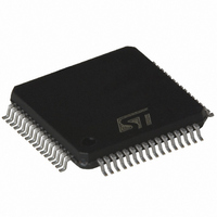
ST7FMC2R6T6 STMicroelectronics, ST7FMC2R6T6 Datasheet - Page 195

ST7FMC2R6T6
Manufacturer Part Number
ST7FMC2R6T6
Description
MCU 8BIT 32K FLASH 64TQFP
Manufacturer
STMicroelectronics
Series
ST7r
Datasheet
1.ST7FMC2S4T6.pdf
(309 pages)
Specifications of ST7FMC2R6T6
Core Processor
ST7
Core Size
8-Bit
Speed
8MHz
Connectivity
LINSCI, SPI
Peripherals
LVD, Motor Control PWM, POR, PWM, WDT
Number Of I /o
44
Program Memory Size
32KB (32K x 8)
Program Memory Type
FLASH
Ram Size
1K x 8
Voltage - Supply (vcc/vdd)
3.8 V ~ 5.5 V
Data Converters
A/D 16x10b
Oscillator Type
Internal
Operating Temperature
-40°C ~ 85°C
Package / Case
64-TQFP, 64-VQFP
Processor Series
ST7FMC2x
Core
ST7
Data Bus Width
8 bit
Data Ram Size
1 KB
Interface Type
SCI, SPI
Maximum Clock Frequency
8 MHz
Number Of Programmable I/os
60
Number Of Timers
3
Maximum Operating Temperature
+ 85 C
Mounting Style
SMD/SMT
Development Tools By Supplier
ST7MC-KIT/BLDC, ST7MDT50-EMU3, STX-RLINK
Minimum Operating Temperature
- 40 C
On-chip Adc
10 bit, 16 Channel
For Use With
497-8402 - BOARD EVAL COMPLETE INVERTER497-8400 - KIT IGBT PWR MODULE CTRL ST7MC497-6408 - BOARD EVAL BLDC SENSORLESS MOTOR497-4734 - EVAL KIT 3KW POWER DRIVER BOARD497-4733 - EVAL KIT 1KW POWER DRIVER BOARD497-4732 - EVAL KIT 300W POWER DRIVER BOARD497-4731 - EVAL KIT PWR DRIVER CONTROL BRD
Lead Free Status / RoHS Status
Lead free / RoHS Compliant
Eeprom Size
-
Lead Free Status / Rohs Status
Details
Other names
497-4868
Available stocks
Company
Part Number
Manufacturer
Quantity
Price
Company:
Part Number:
ST7FMC2R6T6
Manufacturer:
STMicroelectronics
Quantity:
10 000
- Current page: 195 of 309
- Download datasheet (6Mb)
MOTOR CONTROLLER (Cont’d)
Figure 113. Dead Time waveform with delay greater than the positive PWM pulse
Table 52. Dead time programming and example
The deadtime delay is the same for each of the
channels and is programmable with the DTG[5..0]
bits in the MDTG register.
The resolution is variable and depends on the
DTG5 and DTG4 bits.
set-up of the deadtime generator.
IT
put clock (F
ed by the XT16:XT8 prescaler bits in the MCONF
register).
For safety reasons and since the deadtime de-
pends only on external component characteristics
(level-shifter delay, power components switching
duration,...) the register used to set-up deadtime
duration can be written only once after the MCU
reset. This prevents a corrupted program counter
modifying this system critical set-up, which may
cause excessive power dissipation or destructive
shoot-through in the power stage half bridges.
When using the three independent U, V and W
PWM signals (PCN bit set) (see
drive the MCOx outputs, deadtime is added as
shown in
DTG5 DTG4
mtc
0
1
1
Output A
Output B
is the period of the Dead Time Generator in-
Input
Figure
X
0
1
mtc
= 16 MHz in most cases, not affect-
2xT
4xT
8xT
T
111.
dtg
mtc
mtc
mtc
Table 52
Deadtime expression
(DTG[3..0]+17) x T
(DTG[4..0]+1) x T
summarizes the
Figure
114) to
dtg
dtg
From 17 to 32 T
From 1 to 32 T
Deadtime value
The dead time generator is enabled/disabled us-
ing the DTE bit.
The effect of the DTE bit depends on the PCN bit
value.
If the PCN bit is set:
■
■
Note: The reset value of the MDTG register is FFh
so when configuring the dead time, it is mandatory
to follow one the two following sequences:
■
■
DTE is read only. To reset it, first reset the PCN
bit, then reset DTE and set PCN to 1 again.
If DTE=0, the high and low side outputs are
simply complemented (no deadtime insertion,
DTG[5:0] bits are not significant); this is to allow
the use of an external dead time generator.
To use dead t imes while the PCN bit is set; from
reset state write the MDTG value at once. The
DTE bit will be read back as 1 whatever the
programming value (read only if PCN=1)
To use dead times while the PCN bit is reset,
write first the dead time value in DTG[5:0], then
reset the PCN bit, or do both actions at the same
time.
Delay
dtg
dtg
@16MHz F
125ns
250ns
500ns
T
dtg
ST7MC1xx/ST7MC2xx
mtc
Dead time range
@ 16MHz F
0.125µs to 4µs
4.25µs to 8µs
8.5µs to 16µs
5V
0V
5V
0V
5V
0V
195/309
mtc
1
Related parts for ST7FMC2R6T6
Image
Part Number
Description
Manufacturer
Datasheet
Request
R

Part Number:
Description:
STMicroelectronics [RIPPLE-CARRY BINARY COUNTER/DIVIDERS]
Manufacturer:
STMicroelectronics
Datasheet:

Part Number:
Description:
STMicroelectronics [LIQUID-CRYSTAL DISPLAY DRIVERS]
Manufacturer:
STMicroelectronics
Datasheet:

Part Number:
Description:
BOARD EVAL FOR MEMS SENSORS
Manufacturer:
STMicroelectronics
Datasheet:

Part Number:
Description:
NPN TRANSISTOR POWER MODULE
Manufacturer:
STMicroelectronics
Datasheet:

Part Number:
Description:
TURBOSWITCH ULTRA-FAST HIGH VOLTAGE DIODE
Manufacturer:
STMicroelectronics
Datasheet:

Part Number:
Description:
Manufacturer:
STMicroelectronics
Datasheet:

Part Number:
Description:
DIODE / SCR MODULE
Manufacturer:
STMicroelectronics
Datasheet:

Part Number:
Description:
DIODE / SCR MODULE
Manufacturer:
STMicroelectronics
Datasheet:

Part Number:
Description:
Search -----> STE16N100
Manufacturer:
STMicroelectronics
Datasheet:

Part Number:
Description:
Search ---> STE53NA50
Manufacturer:
STMicroelectronics
Datasheet:

Part Number:
Description:
NPN Transistor Power Module
Manufacturer:
STMicroelectronics
Datasheet:

Part Number:
Description:
DIODE / SCR MODULE
Manufacturer:
STMicroelectronics
Datasheet:


