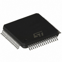
ST7FMC2R6T6 STMicroelectronics, ST7FMC2R6T6 Datasheet - Page 194

ST7FMC2R6T6
Manufacturer Part Number
ST7FMC2R6T6
Description
MCU 8BIT 32K FLASH 64TQFP
Manufacturer
STMicroelectronics
Series
ST7r
Datasheet
1.ST7FMC2S4T6.pdf
(309 pages)
Specifications of ST7FMC2R6T6
Core Processor
ST7
Core Size
8-Bit
Speed
8MHz
Connectivity
LINSCI, SPI
Peripherals
LVD, Motor Control PWM, POR, PWM, WDT
Number Of I /o
44
Program Memory Size
32KB (32K x 8)
Program Memory Type
FLASH
Ram Size
1K x 8
Voltage - Supply (vcc/vdd)
3.8 V ~ 5.5 V
Data Converters
A/D 16x10b
Oscillator Type
Internal
Operating Temperature
-40°C ~ 85°C
Package / Case
64-TQFP, 64-VQFP
Processor Series
ST7FMC2x
Core
ST7
Data Bus Width
8 bit
Data Ram Size
1 KB
Interface Type
SCI, SPI
Maximum Clock Frequency
8 MHz
Number Of Programmable I/os
60
Number Of Timers
3
Maximum Operating Temperature
+ 85 C
Mounting Style
SMD/SMT
Development Tools By Supplier
ST7MC-KIT/BLDC, ST7MDT50-EMU3, STX-RLINK
Minimum Operating Temperature
- 40 C
On-chip Adc
10 bit, 16 Channel
For Use With
497-8402 - BOARD EVAL COMPLETE INVERTER497-8400 - KIT IGBT PWR MODULE CTRL ST7MC497-6408 - BOARD EVAL BLDC SENSORLESS MOTOR497-4734 - EVAL KIT 3KW POWER DRIVER BOARD497-4733 - EVAL KIT 1KW POWER DRIVER BOARD497-4732 - EVAL KIT 300W POWER DRIVER BOARD497-4731 - EVAL KIT PWR DRIVER CONTROL BRD
Lead Free Status / RoHS Status
Lead free / RoHS Compliant
Eeprom Size
-
Lead Free Status / Rohs Status
Details
Other names
497-4868
Available stocks
Company
Part Number
Manufacturer
Quantity
Price
Company:
Part Number:
ST7FMC2R6T6
Manufacturer:
STMicroelectronics
Quantity:
10 000
- Current page: 194 of 309
- Download datasheet (6Mb)
ST7MC1xx/ST7MC2xx
MOTOR CONTROLLER (Cont’d)
10.6.9.3 Dead Time Generator
When using typical triple half bridge topology for
power converters, precautions must be taken to
avoid short circuits in half bridges. This is ensured
by driving high and low side switches with comple-
mentary signals and by managing the time be-
tween the switching-off and the switching-on in-
stants of the adjacent switches.
This time is usually known as deadtime and has to
be adjusted depending on the devices connected
to the PWM outputs and their characteristics (in-
trinsic delays of level-shifters, delays due to power
switches,...).
When driving motors in six-step mode, the dead-
time generator function also allows synchronous
rectification to be performed on the switch adja-
cent to the one where PWM is applied to reduce
conduction losses.
Figure 111. Dead Time waveforms
Figure 112. Dead time waveform with delay greater than the negative PWM pulse
194/309
1
Input signal
Reference
Output A
Output B
Output A
Output B
Input
Delay
For each of the three PWM channels, there is one
6-bit Dead Time generator available.
It generates two output signals: A and B.
The A output signal is the same as the input phase
signal except for the rising edge, which is delayed
relative to the input signal rising edge.
The B output signal is the opposite of the input
phase signal except the rising edge which is de-
layed relative to the input signal falling edge.
Figure 111
output signals of the deadtime register and its in-
puts.
If the delay is greater than the width of the active
phase (A or B) then the corresponding pulse is not
generated (see
Delay
shows the relationship between the
Figure 112
Delay
and
Figure
113).
5V
0V
5V
0V
5V
0V
5V
0V
5V
0V
5V
0V
Related parts for ST7FMC2R6T6
Image
Part Number
Description
Manufacturer
Datasheet
Request
R

Part Number:
Description:
STMicroelectronics [RIPPLE-CARRY BINARY COUNTER/DIVIDERS]
Manufacturer:
STMicroelectronics
Datasheet:

Part Number:
Description:
STMicroelectronics [LIQUID-CRYSTAL DISPLAY DRIVERS]
Manufacturer:
STMicroelectronics
Datasheet:

Part Number:
Description:
BOARD EVAL FOR MEMS SENSORS
Manufacturer:
STMicroelectronics
Datasheet:

Part Number:
Description:
NPN TRANSISTOR POWER MODULE
Manufacturer:
STMicroelectronics
Datasheet:

Part Number:
Description:
TURBOSWITCH ULTRA-FAST HIGH VOLTAGE DIODE
Manufacturer:
STMicroelectronics
Datasheet:

Part Number:
Description:
Manufacturer:
STMicroelectronics
Datasheet:

Part Number:
Description:
DIODE / SCR MODULE
Manufacturer:
STMicroelectronics
Datasheet:

Part Number:
Description:
DIODE / SCR MODULE
Manufacturer:
STMicroelectronics
Datasheet:

Part Number:
Description:
Search -----> STE16N100
Manufacturer:
STMicroelectronics
Datasheet:

Part Number:
Description:
Search ---> STE53NA50
Manufacturer:
STMicroelectronics
Datasheet:

Part Number:
Description:
NPN Transistor Power Module
Manufacturer:
STMicroelectronics
Datasheet:

Part Number:
Description:
DIODE / SCR MODULE
Manufacturer:
STMicroelectronics
Datasheet:


