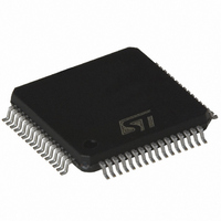
ST7FMC2R6T6 STMicroelectronics, ST7FMC2R6T6 Datasheet - Page 290

ST7FMC2R6T6
Manufacturer Part Number
ST7FMC2R6T6
Description
MCU 8BIT 32K FLASH 64TQFP
Manufacturer
STMicroelectronics
Series
ST7r
Datasheet
1.ST7FMC2S4T6.pdf
(309 pages)
Specifications of ST7FMC2R6T6
Core Processor
ST7
Core Size
8-Bit
Speed
8MHz
Connectivity
LINSCI, SPI
Peripherals
LVD, Motor Control PWM, POR, PWM, WDT
Number Of I /o
44
Program Memory Size
32KB (32K x 8)
Program Memory Type
FLASH
Ram Size
1K x 8
Voltage - Supply (vcc/vdd)
3.8 V ~ 5.5 V
Data Converters
A/D 16x10b
Oscillator Type
Internal
Operating Temperature
-40°C ~ 85°C
Package / Case
64-TQFP, 64-VQFP
Processor Series
ST7FMC2x
Core
ST7
Data Bus Width
8 bit
Data Ram Size
1 KB
Interface Type
SCI, SPI
Maximum Clock Frequency
8 MHz
Number Of Programmable I/os
60
Number Of Timers
3
Maximum Operating Temperature
+ 85 C
Mounting Style
SMD/SMT
Development Tools By Supplier
ST7MC-KIT/BLDC, ST7MDT50-EMU3, STX-RLINK
Minimum Operating Temperature
- 40 C
On-chip Adc
10 bit, 16 Channel
For Use With
497-8402 - BOARD EVAL COMPLETE INVERTER497-8400 - KIT IGBT PWR MODULE CTRL ST7MC497-6408 - BOARD EVAL BLDC SENSORLESS MOTOR497-4734 - EVAL KIT 3KW POWER DRIVER BOARD497-4733 - EVAL KIT 1KW POWER DRIVER BOARD497-4732 - EVAL KIT 300W POWER DRIVER BOARD497-4731 - EVAL KIT PWR DRIVER CONTROL BRD
Lead Free Status / RoHS Status
Lead free / RoHS Compliant
Eeprom Size
-
Lead Free Status / Rohs Status
Details
Other names
497-4868
Available stocks
Company
Part Number
Manufacturer
Quantity
Price
Company:
Part Number:
ST7FMC2R6T6
Manufacturer:
STMicroelectronics
Quantity:
10 000
- Current page: 290 of 309
- Download datasheet (6Mb)
ST7MC1xx/ST7MC2xx
14 ST7MC DEVICE CONFIGURATION AND ORDERING INFORMATION
Each device is available for production in ROM
versions and in user programmable versions
(FLASH) as well as in factory coded versions
(FASTROM). ST7MC are ROM devices. ST7PMC
devices are Factory Advanced Service Technique
ROM (FASTROM) versions: they are programmed
Flash devices.
14.1 FLASH OPTION BYTES
The option bytes allow the hardware configuration
of the microcontroller to be selected. They have no
address in the memory map and can be accessed
only in programming mode (for example using a
standard ST7 programming tool). The default con-
tent of the FLASH is fixed to FFh. This means that
all the options have “1” as their default value.
OPTION BYTE 0
OPT7= WDG HALT Watchdog and Halt mode
This option bit determines if a RESET is generated
when entering Halt mode while the Watchdog is
active.
0: No Reset generation when entering Halt mode
1: Reset generation when entering Halt mode
OPT6= WDG SW Hardware or software watchdog
This option bit selects the watchdog type.
0: Hardware (watchdog always enabled)
1: Software (watchdog to be enabled by software)
OPT5 = CKSEL Clock Source Selection.
0: PLL clock selected
1: Oscillator clock selected
Note 1: Even if PLL clock is selected, a clock signal must
always be present (refer to
OPT4:3= VD[1:0] Voltage detection
These option bits enable the voltage detection
block (LVD, and AVD).
290/309
Default
value
Selected Low Voltage Detector
LVD On and AVD Off
7
LVD and AVD On
1
WDG
1
STATIC OPTION BYTE 0
1)
1
Figure 13. on page
1
1
VD
0
1
VD1
0
0
1
28)
VD0
1
0
1
1
0
ST7FMC Flash devices are shipped to customers
with a default content (FFh), while ROM/FAS-
TROM factory coded parts contain the code sup-
plied by the customer. This implies that Flash de-
vices have to be configured by the customer using
the Option Bytes while the ROM devices are facto-
ry-configured.
OPT2 = RSTC RESET clock cycle selection
This option bit selects the number of CPU cycles
applied during the RESET phase and when exiting
Halt mode. For resonator oscillators, it is advised
to select 4096 due to the long crystal stabilization
time.
0: Reset phase with 4096 CPU cycles
1: Reset phase with 256 CPU cycles
Note: When the PLL clock is selected (CKSEL=0),
the reset clock cycle selection is forced to 4096
CPU cycles.
OPT1= DIV2 Divider by 2
1: DIV2 divider disabled with OSCIN = 8MHz
0: DIV2 divider enabled (in order to have 8 MHz re-
OPT0= FMP_R Flash memory read-out protection
Readout protection, when selected provides a pro-
tection against program memory content extrac-
tion and against write access to Flash memory.
This protection is based on a read/write protection
of the memory in test modes and ICP mode. Eras-
ing the option bytes when the FMP_R option is se-
lected causes the whole user memory to be
erased first and the device can be reprogrammed.
Refer to the ST7 Flash Programming Reference
Manual and
tails.
0: Read-out protection enabled
1: Read-out protection disabled
quired for the PLL with OSCIN =16 Mhz))
2
1
7
Selected Low Voltage Detector
PKG
1
1
LVD and AVD Off
section 4.3.1 on page 22
STATIC OPTION BYTE 1
0
1
1
1
1
VD1
for more de-
1
1
1
MCO
VD0
0
0
1
1
Related parts for ST7FMC2R6T6
Image
Part Number
Description
Manufacturer
Datasheet
Request
R

Part Number:
Description:
STMicroelectronics [RIPPLE-CARRY BINARY COUNTER/DIVIDERS]
Manufacturer:
STMicroelectronics
Datasheet:

Part Number:
Description:
STMicroelectronics [LIQUID-CRYSTAL DISPLAY DRIVERS]
Manufacturer:
STMicroelectronics
Datasheet:

Part Number:
Description:
BOARD EVAL FOR MEMS SENSORS
Manufacturer:
STMicroelectronics
Datasheet:

Part Number:
Description:
NPN TRANSISTOR POWER MODULE
Manufacturer:
STMicroelectronics
Datasheet:

Part Number:
Description:
TURBOSWITCH ULTRA-FAST HIGH VOLTAGE DIODE
Manufacturer:
STMicroelectronics
Datasheet:

Part Number:
Description:
Manufacturer:
STMicroelectronics
Datasheet:

Part Number:
Description:
DIODE / SCR MODULE
Manufacturer:
STMicroelectronics
Datasheet:

Part Number:
Description:
DIODE / SCR MODULE
Manufacturer:
STMicroelectronics
Datasheet:

Part Number:
Description:
Search -----> STE16N100
Manufacturer:
STMicroelectronics
Datasheet:

Part Number:
Description:
Search ---> STE53NA50
Manufacturer:
STMicroelectronics
Datasheet:

Part Number:
Description:
NPN Transistor Power Module
Manufacturer:
STMicroelectronics
Datasheet:

Part Number:
Description:
DIODE / SCR MODULE
Manufacturer:
STMicroelectronics
Datasheet:


