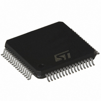
ST7FMC2R6T6 STMicroelectronics, ST7FMC2R6T6 Datasheet - Page 204

ST7FMC2R6T6
Manufacturer Part Number
ST7FMC2R6T6
Description
MCU 8BIT 32K FLASH 64TQFP
Manufacturer
STMicroelectronics
Series
ST7r
Datasheet
1.ST7FMC2S4T6.pdf
(309 pages)
Specifications of ST7FMC2R6T6
Core Processor
ST7
Core Size
8-Bit
Speed
8MHz
Connectivity
LINSCI, SPI
Peripherals
LVD, Motor Control PWM, POR, PWM, WDT
Number Of I /o
44
Program Memory Size
32KB (32K x 8)
Program Memory Type
FLASH
Ram Size
1K x 8
Voltage - Supply (vcc/vdd)
3.8 V ~ 5.5 V
Data Converters
A/D 16x10b
Oscillator Type
Internal
Operating Temperature
-40°C ~ 85°C
Package / Case
64-TQFP, 64-VQFP
Processor Series
ST7FMC2x
Core
ST7
Data Bus Width
8 bit
Data Ram Size
1 KB
Interface Type
SCI, SPI
Maximum Clock Frequency
8 MHz
Number Of Programmable I/os
60
Number Of Timers
3
Maximum Operating Temperature
+ 85 C
Mounting Style
SMD/SMT
Development Tools By Supplier
ST7MC-KIT/BLDC, ST7MDT50-EMU3, STX-RLINK
Minimum Operating Temperature
- 40 C
On-chip Adc
10 bit, 16 Channel
For Use With
497-8402 - BOARD EVAL COMPLETE INVERTER497-8400 - KIT IGBT PWR MODULE CTRL ST7MC497-6408 - BOARD EVAL BLDC SENSORLESS MOTOR497-4734 - EVAL KIT 3KW POWER DRIVER BOARD497-4733 - EVAL KIT 1KW POWER DRIVER BOARD497-4732 - EVAL KIT 300W POWER DRIVER BOARD497-4731 - EVAL KIT PWR DRIVER CONTROL BRD
Lead Free Status / RoHS Status
Lead free / RoHS Compliant
Eeprom Size
-
Lead Free Status / Rohs Status
Details
Other names
497-4868
Available stocks
Company
Part Number
Manufacturer
Quantity
Price
Company:
Part Number:
ST7FMC2R6T6
Manufacturer:
STMicroelectronics
Quantity:
10 000
- Current page: 204 of 309
- Download datasheet (6Mb)
ST7MC1xx/ST7MC2xx
MOTOR CONTROLLER (Cont’d)
■
This mode is useful for MCMP0 values ranging
from 9 bits to 12 bits.
Compare 0 and Compare U, V, W should be load-
ed). It requires loading two bytes in the MCMPxH
and MCMPxL registers (i.e. MCMP0, MCMPU,
MCMPV and MCMPW 16-bit registers) following
the sequence described below:
– write to the MCMPxL register (LSB) first
– then write to the MCMPxH register (MSB).
The 16-bit value is then ready to be transferred in
the active register as soon as an update event oc-
curs. This sequence is necessary to avoid poten-
tial conflicts with update interrupts causing the
hardware transfer from preload to active registers:
if an update event occurs in the middle of the
above sequence, the update is effective only when
the MSB has been written.
■
This mode is useful whenever the MCMP0 value is
less or equal to 8-bits. It allows significant CPU re-
Figure 121. Comparison between 12-bit and 8-bit PWM mode
204/309
1
12-bit PWM mode
12-bit Mode (PMS bit = 0 in the MPCR register)
8-bit PWM mode (PMS bit = 1 in MPCR register)
8-bit PWM mode
(PMS bit = 0)
(PMS bit = 1)
Figure 121
OvfX
MCMP0H
MCMPxH
MCMP0H
MCMPxH
Ext
b7
b7
b7
b7
MPCR
b7
OvfU
presents the way
OvfV
OvfW
b0
b0
b0
b0
b0
source savings when computing three-phase duty
cycles during PWM interrupt routines. In this
mode, the Compare 0 and Compare U, V, W reg-
isters have the same size (8 bits). The extension of
the MCMPx registers is done in using the OVFx
bits in the MPCR register (refer to
These bits force the related duty-cycles to 100%
and are reset by hardware on occurence of a
PWM update event.
Note about read access to registers with
preload: during read accesses, values read are
the content of the preload registers, not the active
registers.
Note about compare register active bit loca-
tions: the 13 active bits of the MCMPx registers
are left-aligned. This allows temporary calculations
to be done with 16-bit precision, round-up is done
automatically to the 13-bit format when loading the
values of the MCMPx registers.
Note about MCMP0x registers: the configuration
MCMP0H=MCMP0L=0 is not allowed
MCMP0L
MCMPxL
MCMP0L
MCMPxL
b7
b7
b7
b7
Ext
Equivalent bit location
Bit extending comparison range
Bit not available
b0
b0
b0
b0
PWM frequency
PWM frequency
Phase x duty
Phase x duty
cycle set-up
cycle set-up
set-up
set-up
Figure
121).
Related parts for ST7FMC2R6T6
Image
Part Number
Description
Manufacturer
Datasheet
Request
R

Part Number:
Description:
STMicroelectronics [RIPPLE-CARRY BINARY COUNTER/DIVIDERS]
Manufacturer:
STMicroelectronics
Datasheet:

Part Number:
Description:
STMicroelectronics [LIQUID-CRYSTAL DISPLAY DRIVERS]
Manufacturer:
STMicroelectronics
Datasheet:

Part Number:
Description:
BOARD EVAL FOR MEMS SENSORS
Manufacturer:
STMicroelectronics
Datasheet:

Part Number:
Description:
NPN TRANSISTOR POWER MODULE
Manufacturer:
STMicroelectronics
Datasheet:

Part Number:
Description:
TURBOSWITCH ULTRA-FAST HIGH VOLTAGE DIODE
Manufacturer:
STMicroelectronics
Datasheet:

Part Number:
Description:
Manufacturer:
STMicroelectronics
Datasheet:

Part Number:
Description:
DIODE / SCR MODULE
Manufacturer:
STMicroelectronics
Datasheet:

Part Number:
Description:
DIODE / SCR MODULE
Manufacturer:
STMicroelectronics
Datasheet:

Part Number:
Description:
Search -----> STE16N100
Manufacturer:
STMicroelectronics
Datasheet:

Part Number:
Description:
Search ---> STE53NA50
Manufacturer:
STMicroelectronics
Datasheet:

Part Number:
Description:
NPN Transistor Power Module
Manufacturer:
STMicroelectronics
Datasheet:

Part Number:
Description:
DIODE / SCR MODULE
Manufacturer:
STMicroelectronics
Datasheet:


