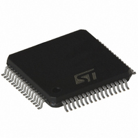
ST7FMC2R6T6 STMicroelectronics, ST7FMC2R6T6 Datasheet - Page 132

ST7FMC2R6T6
Manufacturer Part Number
ST7FMC2R6T6
Description
MCU 8BIT 32K FLASH 64TQFP
Manufacturer
STMicroelectronics
Series
ST7r
Datasheet
1.ST7FMC2S4T6.pdf
(309 pages)
Specifications of ST7FMC2R6T6
Core Processor
ST7
Core Size
8-Bit
Speed
8MHz
Connectivity
LINSCI, SPI
Peripherals
LVD, Motor Control PWM, POR, PWM, WDT
Number Of I /o
44
Program Memory Size
32KB (32K x 8)
Program Memory Type
FLASH
Ram Size
1K x 8
Voltage - Supply (vcc/vdd)
3.8 V ~ 5.5 V
Data Converters
A/D 16x10b
Oscillator Type
Internal
Operating Temperature
-40°C ~ 85°C
Package / Case
64-TQFP, 64-VQFP
Processor Series
ST7FMC2x
Core
ST7
Data Bus Width
8 bit
Data Ram Size
1 KB
Interface Type
SCI, SPI
Maximum Clock Frequency
8 MHz
Number Of Programmable I/os
60
Number Of Timers
3
Maximum Operating Temperature
+ 85 C
Mounting Style
SMD/SMT
Development Tools By Supplier
ST7MC-KIT/BLDC, ST7MDT50-EMU3, STX-RLINK
Minimum Operating Temperature
- 40 C
On-chip Adc
10 bit, 16 Channel
For Use With
497-8402 - BOARD EVAL COMPLETE INVERTER497-8400 - KIT IGBT PWR MODULE CTRL ST7MC497-6408 - BOARD EVAL BLDC SENSORLESS MOTOR497-4734 - EVAL KIT 3KW POWER DRIVER BOARD497-4733 - EVAL KIT 1KW POWER DRIVER BOARD497-4732 - EVAL KIT 300W POWER DRIVER BOARD497-4731 - EVAL KIT PWR DRIVER CONTROL BRD
Lead Free Status / RoHS Status
Lead free / RoHS Compliant
Eeprom Size
-
Lead Free Status / Rohs Status
Details
Other names
497-4868
Available stocks
Company
Part Number
Manufacturer
Quantity
Price
Company:
Part Number:
ST7FMC2R6T6
Manufacturer:
STMicroelectronics
Quantity:
10 000
- Current page: 132 of 309
- Download datasheet (6Mb)
ST7MC1xx/ST7MC2xx
LINSCI™ SERIAL COMMUNICATION INTERFACE (LIN Mode) (cont’d)
10.5.10 LIN Mode Register Description
STATUS REGISTER (SCISR)
Read Only
Reset Value: 1100 0000 (C0h)
Bits 7:4 = Same function as in SCI mode, please
refer to
scription.
Bit 3 = LHE LIN Header Error.
During LIN Header this bit signals three error
types:
– The LIN Synch Field is corrupted and the SCI is
– A timeout occurred during LIN Header reception
– An overrun error was detected on one of the
An interrupt is generated if RIE = 1 in the SCICR2
register. If blocked in the LIN Synch State, the LSF
bit must first be reset (to exit LIN Synch Field state
and then to be able to clear LHE flag). Then it is
cleared by the following software sequence: An
access to the SCISR register followed by a read to
the SCIDR register.
0: No LIN Header error
1: LIN Header error detected
Note:
Apart from the LIN Header this bit signals an Over-
run Error as in SCI mode, (see description in
tion 10.5.8 SCI Mode Register
Bit 2 = NF Noise flag
In LIN Master mode (LINE bit = 1 and LSLV bit = 0)
this bit has the same function as in SCI mode,
please refer to
Description
In LIN Slave mode (LINE bit = 1 and LSLV bit = 1)
this bit has no meaning.
Bit 1 = FE Framing error.
In LIN slave mode, this bit is set only when a real
132/309
1
TDRE
blocked in LIN Synch State (LSF bit = 1).
header field (see OR bit description in
10.5.8 SCI Mode Register
7
TC
Section 10.5.8 SCI Mode Register De-
RDRF
Section 10.5.8 SCI Mode Register
IDLE
LHE
Description)).
Description)
NF
FE
Section
Sec-
PE
0
framing error is detected (if the stop bit is dominant
(0) and at least one of the other bits is recessive
(1). It is not set when a break occurs, the LHDF bit
is used instead as a break flag (if the LHDM
bit = 0). It is cleared by a software sequence (an
access to the SCISR register followed by a read to
the SCIDR register).
0: No Framing error
1: Framing error detected
Bit 0 = PE Parity error.
This bit is set by hardware when a LIN parity error
occurs (if the PCE bit is set) in receiver mode. It is
cleared by a software sequence (a read to the sta-
tus register followed by an access to the SCIDR
data register). An interrupt is generated if PIE = 1
in the SCICR1 register.
0: No LIN parity error
1: LIN Parity error detected
CONTROL REGISTER 1 (SCICR1)
Read/Write
Reset Value: x000 0000 (x0h)
Bits 7:3 = Same function as in SCI mode, please
refer to
scription.
Bit 2 = PCE Parity control enable.
This bit is set and cleared by software. It selects
the hardware parity control for LIN identifier parity
check.
0: Parity control disabled
1: Parity control enabled
When a parity error occurs, the PE bit in the
SCISR register is set.
Bit 1 = Reserved
Bit 0 = Same function as in SCI mode, please refer
to
R8
Section 10.5.8 SCI Mode Register
7
T8
Section 10.5.8 SCI Mode Register De-
SCID
M
WAKE
PCE
Description.
PS
PIE
0
Related parts for ST7FMC2R6T6
Image
Part Number
Description
Manufacturer
Datasheet
Request
R

Part Number:
Description:
STMicroelectronics [RIPPLE-CARRY BINARY COUNTER/DIVIDERS]
Manufacturer:
STMicroelectronics
Datasheet:

Part Number:
Description:
STMicroelectronics [LIQUID-CRYSTAL DISPLAY DRIVERS]
Manufacturer:
STMicroelectronics
Datasheet:

Part Number:
Description:
BOARD EVAL FOR MEMS SENSORS
Manufacturer:
STMicroelectronics
Datasheet:

Part Number:
Description:
NPN TRANSISTOR POWER MODULE
Manufacturer:
STMicroelectronics
Datasheet:

Part Number:
Description:
TURBOSWITCH ULTRA-FAST HIGH VOLTAGE DIODE
Manufacturer:
STMicroelectronics
Datasheet:

Part Number:
Description:
Manufacturer:
STMicroelectronics
Datasheet:

Part Number:
Description:
DIODE / SCR MODULE
Manufacturer:
STMicroelectronics
Datasheet:

Part Number:
Description:
DIODE / SCR MODULE
Manufacturer:
STMicroelectronics
Datasheet:

Part Number:
Description:
Search -----> STE16N100
Manufacturer:
STMicroelectronics
Datasheet:

Part Number:
Description:
Search ---> STE53NA50
Manufacturer:
STMicroelectronics
Datasheet:

Part Number:
Description:
NPN Transistor Power Module
Manufacturer:
STMicroelectronics
Datasheet:

Part Number:
Description:
DIODE / SCR MODULE
Manufacturer:
STMicroelectronics
Datasheet:


