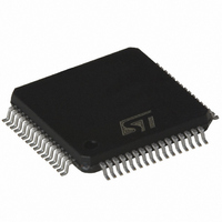
ST7FMC2R6T6 STMicroelectronics, ST7FMC2R6T6 Datasheet - Page 264

ST7FMC2R6T6
Manufacturer Part Number
ST7FMC2R6T6
Description
MCU 8BIT 32K FLASH 64TQFP
Manufacturer
STMicroelectronics
Series
ST7r
Datasheet
1.ST7FMC2S4T6.pdf
(309 pages)
Specifications of ST7FMC2R6T6
Core Processor
ST7
Core Size
8-Bit
Speed
8MHz
Connectivity
LINSCI, SPI
Peripherals
LVD, Motor Control PWM, POR, PWM, WDT
Number Of I /o
44
Program Memory Size
32KB (32K x 8)
Program Memory Type
FLASH
Ram Size
1K x 8
Voltage - Supply (vcc/vdd)
3.8 V ~ 5.5 V
Data Converters
A/D 16x10b
Oscillator Type
Internal
Operating Temperature
-40°C ~ 85°C
Package / Case
64-TQFP, 64-VQFP
Processor Series
ST7FMC2x
Core
ST7
Data Bus Width
8 bit
Data Ram Size
1 KB
Interface Type
SCI, SPI
Maximum Clock Frequency
8 MHz
Number Of Programmable I/os
60
Number Of Timers
3
Maximum Operating Temperature
+ 85 C
Mounting Style
SMD/SMT
Development Tools By Supplier
ST7MC-KIT/BLDC, ST7MDT50-EMU3, STX-RLINK
Minimum Operating Temperature
- 40 C
On-chip Adc
10 bit, 16 Channel
For Use With
497-8402 - BOARD EVAL COMPLETE INVERTER497-8400 - KIT IGBT PWR MODULE CTRL ST7MC497-6408 - BOARD EVAL BLDC SENSORLESS MOTOR497-4734 - EVAL KIT 3KW POWER DRIVER BOARD497-4733 - EVAL KIT 1KW POWER DRIVER BOARD497-4732 - EVAL KIT 300W POWER DRIVER BOARD497-4731 - EVAL KIT PWR DRIVER CONTROL BRD
Lead Free Status / RoHS Status
Lead free / RoHS Compliant
Eeprom Size
-
Lead Free Status / Rohs Status
Details
Other names
497-4868
Available stocks
Company
Part Number
Manufacturer
Quantity
Price
Company:
Part Number:
ST7FMC2R6T6
Manufacturer:
STMicroelectronics
Quantity:
10 000
- Current page: 264 of 309
- Download datasheet (6Mb)
ST7MC1xx/ST7MC2xx
12.8 I/O PORT PIN CHARACTERISTICS
12.8.1 General Characteristics
Subject to general operating conditions for V
Notes:
1. Data based on characterization results, not tested in production.
2. Hysteresis voltage between Schmitt trigger switching levels. Based on characterization results, not tested.
3. I
respected, the injection current must be limited externally to the I
while a negative injection is induced by V
Refer to
4. Configuration not recommended, all unused pins must be kept at a fixed voltage: using the output mode of the I/O for
example or an external pull-up or pull-down resistor (see
based on design simulation and technology characteristics, not tested in production. This value depends on V
perature values.
5. The R
scribed in
6. To generate an external interrupt, a minimum pulse width has to be applied on an I/O port pin configured as an external
interrupt source.
264/309
ΣI
I
Symbol
INJ(PIN)
t
t
t
INJ(PIN)
r(IO)out
f(IO)out
w(IT)in
INJ(PIN)
V
V
R
C
V
V
V
V
I
I
hys
hys
PU
)
S
IH
IH
L
IO
IL
IL
3)
section 12.2.2 on page 248
PU
3
Figure
must never be exceeded. This is implicitly insured if V
pull-up equivalent resistor is based on a resistive transistor (corresponding I
Input low level voltage
Input high level voltage
Schmitt trigger voltage hysteresis
Input low level voltage
Input high level voltage
Schmitt trigger voltage hysteresis
Injected Current on an I/O
Total injected current (sum of all I/O
and control pins)
Input leakage current
Static current consumption induced
by each floating input pin
Weak pull-up equivalent resistor
I/O pin capacitance
Output high to low level fall time
Output low to high level rise time
External interrupt pulse time
139). This data is based on characterization results, tested in production at V
Parameter
for more details. For PD7, refer to ‘INJECTED CURRENT ON PD7” on
4)
6)
IN
<V
1)
5)
1)
SS
2)
2)
.
CMOS ports
G & H ports
V
V
Floating input mode
V
C
Between 10% and 90%
DD
DD
SS
IN
L
=50pF
=
≤
=5V
V
, f
V
IN
SS
OSC
Figure
Conditions
≤
V
DD
, and T
138). Static peak current value taken at a fixed V
INJ(PIN)
IN
maximum is respected. If V
A
unless otherwise specified.
value. A positive injection is induced by V
0.7xV
Min
2.8
50
1
DD
PU
Typ
400
200
90
25
25
1
5
current characteristics de-
DD
IN
max.
maximum cannot be
0.3xV
+5/-2
Max
± 25
250
0.8
±1
DD
DD
page
and tem-
IN
IN
t
Unit
mV
mA
CPU
μA
pF
kΩ
ns
value,
V
V
V
>V
303.
DD
Related parts for ST7FMC2R6T6
Image
Part Number
Description
Manufacturer
Datasheet
Request
R

Part Number:
Description:
STMicroelectronics [RIPPLE-CARRY BINARY COUNTER/DIVIDERS]
Manufacturer:
STMicroelectronics
Datasheet:

Part Number:
Description:
STMicroelectronics [LIQUID-CRYSTAL DISPLAY DRIVERS]
Manufacturer:
STMicroelectronics
Datasheet:

Part Number:
Description:
BOARD EVAL FOR MEMS SENSORS
Manufacturer:
STMicroelectronics
Datasheet:

Part Number:
Description:
NPN TRANSISTOR POWER MODULE
Manufacturer:
STMicroelectronics
Datasheet:

Part Number:
Description:
TURBOSWITCH ULTRA-FAST HIGH VOLTAGE DIODE
Manufacturer:
STMicroelectronics
Datasheet:

Part Number:
Description:
Manufacturer:
STMicroelectronics
Datasheet:

Part Number:
Description:
DIODE / SCR MODULE
Manufacturer:
STMicroelectronics
Datasheet:

Part Number:
Description:
DIODE / SCR MODULE
Manufacturer:
STMicroelectronics
Datasheet:

Part Number:
Description:
Search -----> STE16N100
Manufacturer:
STMicroelectronics
Datasheet:

Part Number:
Description:
Search ---> STE53NA50
Manufacturer:
STMicroelectronics
Datasheet:

Part Number:
Description:
NPN Transistor Power Module
Manufacturer:
STMicroelectronics
Datasheet:

Part Number:
Description:
DIODE / SCR MODULE
Manufacturer:
STMicroelectronics
Datasheet:


