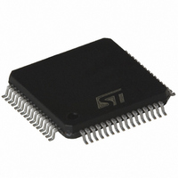
ST7FMC2R6T6 STMicroelectronics, ST7FMC2R6T6 Datasheet - Page 223

ST7FMC2R6T6
Manufacturer Part Number
ST7FMC2R6T6
Description
MCU 8BIT 32K FLASH 64TQFP
Manufacturer
STMicroelectronics
Series
ST7r
Datasheet
1.ST7FMC2S4T6.pdf
(309 pages)
Specifications of ST7FMC2R6T6
Core Processor
ST7
Core Size
8-Bit
Speed
8MHz
Connectivity
LINSCI, SPI
Peripherals
LVD, Motor Control PWM, POR, PWM, WDT
Number Of I /o
44
Program Memory Size
32KB (32K x 8)
Program Memory Type
FLASH
Ram Size
1K x 8
Voltage - Supply (vcc/vdd)
3.8 V ~ 5.5 V
Data Converters
A/D 16x10b
Oscillator Type
Internal
Operating Temperature
-40°C ~ 85°C
Package / Case
64-TQFP, 64-VQFP
Processor Series
ST7FMC2x
Core
ST7
Data Bus Width
8 bit
Data Ram Size
1 KB
Interface Type
SCI, SPI
Maximum Clock Frequency
8 MHz
Number Of Programmable I/os
60
Number Of Timers
3
Maximum Operating Temperature
+ 85 C
Mounting Style
SMD/SMT
Development Tools By Supplier
ST7MC-KIT/BLDC, ST7MDT50-EMU3, STX-RLINK
Minimum Operating Temperature
- 40 C
On-chip Adc
10 bit, 16 Channel
For Use With
497-8402 - BOARD EVAL COMPLETE INVERTER497-8400 - KIT IGBT PWR MODULE CTRL ST7MC497-6408 - BOARD EVAL BLDC SENSORLESS MOTOR497-4734 - EVAL KIT 3KW POWER DRIVER BOARD497-4733 - EVAL KIT 1KW POWER DRIVER BOARD497-4732 - EVAL KIT 300W POWER DRIVER BOARD497-4731 - EVAL KIT PWR DRIVER CONTROL BRD
Lead Free Status / RoHS Status
Lead free / RoHS Compliant
Eeprom Size
-
Lead Free Status / Rohs Status
Details
Other names
497-4868
Available stocks
Company
Part Number
Manufacturer
Quantity
Price
Company:
Part Number:
ST7FMC2R6T6
Manufacturer:
STMicroelectronics
Quantity:
10 000
- Current page: 223 of 309
- Download datasheet (6Mb)
MOTOR CONTROLLER (Cont’d)
PWM REGISTER (MPWME)
Read/Write
Reset Value: 0000 0000 (00h)
Bit 7 = DG:Debug Option.
This bit is used to enter debug mode. As a result,
C, D and Z events are output on 2 pins MCDEM
and MCZEM in Switched and Autoswitched mode,
C and U events are output in Speed Measurement
mode. Refer to
more details
0: Normal mode
1: Debug mode
Bit 6 = PWMW: PWM W output control
0: PWM on Compare Register W is not output on
1: PWM on Compare Register W is output on
Bit 5 = PWMV: PWM V output control
0: PWM on Compare Register V is not output on
1: PWM on Compare Register V is output on MCP-
Bit 4 = PWMU: PWM U output control
0: PWM on Compare Register U is not output on
1: PWM on Compare Register U is output on
DG
MCPWMW pin
MCPWMW pin
MCPWMV pin
WMV pin
MCPWMU pin
MCPWMU pin
7
PWMW PWMV PWMU
6
5
section10.6.7.3 on page 172
4
OT3
3
OT2
2
OT1
1
OT0
0
for
Bits 3:0 = OT[3:0]: Off Time selection
These bits are used to select the OFF time in sen-
sorless current mode as shown in the following ta-
ble.
Table 76. OFF time bits
Note: Times are indicated for 4 MHz f
OT3 OT2 OT1 OT0
0
0
0
0
0
0
0
0
1
1
1
1
1
1
1
1
0
0
0
0
1
1
1
1
0
0
0
0
1
1
1
1
0
0
1
1
0
0
1
1
0
0
1
1
0
0
1
1
0
1
0
1
0
1
0
1
0
1
0
1
0
1
0
1
sorless mode
Off Time sen-
(DS[3:0]=0)
32.5
37.5
12.5 µs
17.5 µs
22.5 µs
27.5 µs
(SR=0)
2.5 µs
7.5 µs
35
40
10 µs
15 µs
20 µs
25 µs
30 µs
ST7MC1xx/ST7MC2xx
5 µs
μs
μs
μs
μs
pling during ON
No minimum off -
(SR=1) or sam-
and/or DS [3:0]
ime in sensor-
less (SPLG =1
Sensor Mode
PERIPH
bits)
time
223/309
Related parts for ST7FMC2R6T6
Image
Part Number
Description
Manufacturer
Datasheet
Request
R

Part Number:
Description:
STMicroelectronics [RIPPLE-CARRY BINARY COUNTER/DIVIDERS]
Manufacturer:
STMicroelectronics
Datasheet:

Part Number:
Description:
STMicroelectronics [LIQUID-CRYSTAL DISPLAY DRIVERS]
Manufacturer:
STMicroelectronics
Datasheet:

Part Number:
Description:
BOARD EVAL FOR MEMS SENSORS
Manufacturer:
STMicroelectronics
Datasheet:

Part Number:
Description:
NPN TRANSISTOR POWER MODULE
Manufacturer:
STMicroelectronics
Datasheet:

Part Number:
Description:
TURBOSWITCH ULTRA-FAST HIGH VOLTAGE DIODE
Manufacturer:
STMicroelectronics
Datasheet:

Part Number:
Description:
Manufacturer:
STMicroelectronics
Datasheet:

Part Number:
Description:
DIODE / SCR MODULE
Manufacturer:
STMicroelectronics
Datasheet:

Part Number:
Description:
DIODE / SCR MODULE
Manufacturer:
STMicroelectronics
Datasheet:

Part Number:
Description:
Search -----> STE16N100
Manufacturer:
STMicroelectronics
Datasheet:

Part Number:
Description:
Search ---> STE53NA50
Manufacturer:
STMicroelectronics
Datasheet:

Part Number:
Description:
NPN Transistor Power Module
Manufacturer:
STMicroelectronics
Datasheet:

Part Number:
Description:
DIODE / SCR MODULE
Manufacturer:
STMicroelectronics
Datasheet:


