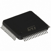
ST7FMC2R6T6 STMicroelectronics, ST7FMC2R6T6 Datasheet - Page 164

ST7FMC2R6T6
Manufacturer Part Number
ST7FMC2R6T6
Description
MCU 8BIT 32K FLASH 64TQFP
Manufacturer
STMicroelectronics
Series
ST7r
Datasheet
1.ST7FMC2S4T6.pdf
(309 pages)
Specifications of ST7FMC2R6T6
Core Processor
ST7
Core Size
8-Bit
Speed
8MHz
Connectivity
LINSCI, SPI
Peripherals
LVD, Motor Control PWM, POR, PWM, WDT
Number Of I /o
44
Program Memory Size
32KB (32K x 8)
Program Memory Type
FLASH
Ram Size
1K x 8
Voltage - Supply (vcc/vdd)
3.8 V ~ 5.5 V
Data Converters
A/D 16x10b
Oscillator Type
Internal
Operating Temperature
-40°C ~ 85°C
Package / Case
64-TQFP, 64-VQFP
Processor Series
ST7FMC2x
Core
ST7
Data Bus Width
8 bit
Data Ram Size
1 KB
Interface Type
SCI, SPI
Maximum Clock Frequency
8 MHz
Number Of Programmable I/os
60
Number Of Timers
3
Maximum Operating Temperature
+ 85 C
Mounting Style
SMD/SMT
Development Tools By Supplier
ST7MC-KIT/BLDC, ST7MDT50-EMU3, STX-RLINK
Minimum Operating Temperature
- 40 C
On-chip Adc
10 bit, 16 Channel
For Use With
497-8402 - BOARD EVAL COMPLETE INVERTER497-8400 - KIT IGBT PWR MODULE CTRL ST7MC497-6408 - BOARD EVAL BLDC SENSORLESS MOTOR497-4734 - EVAL KIT 3KW POWER DRIVER BOARD497-4733 - EVAL KIT 1KW POWER DRIVER BOARD497-4732 - EVAL KIT 300W POWER DRIVER BOARD497-4731 - EVAL KIT PWR DRIVER CONTROL BRD
Lead Free Status / RoHS Status
Lead free / RoHS Compliant
Eeprom Size
-
Lead Free Status / Rohs Status
Details
Other names
497-4868
Available stocks
Company
Part Number
Manufacturer
Quantity
Price
Company:
Part Number:
ST7FMC2R6T6
Manufacturer:
STMicroelectronics
Quantity:
10 000
- Current page: 164 of 309
- Download datasheet (6Mb)
ST7MC1xx/ST7MC2xx
MOTOR CONTROLLER (Cont’d)
10.6.6.11 Speed Sensor Mode
This mode is entered whenever the Tacho Edge
Selection bits in the MPAR register are not both re-
set (TES[1:0] = 01, 10 or 11). The corresponding
block diagram is shown in
Either Incremental Encoder or Tachogenerator-
type speed sensor can be selected with the IS[1:0]
bits in the MPHST register.
10.6.6.12 Tachogenerator Mode (IS[1:0] = 00, 01
or 10)
Any of the MCIx input pins can be used as a tacho-
generator input, with a digital signal (externally
amplified for instance); the two remaining pins can
be used as standard I/O ports.
A digital multiplexer connects the chosen MCIx in-
put to an edge detection block. Input selection is
done with the IS[1:0] bits in the MPHST register.
An edge selection block is used to select one of
three ways to trigger capture events: rising edge,
falling edge or both rising and falling edge sensi-
Figure 88. Input Stage in Speed Sensor Mode (TES[1:0] bits = 01, 10, 11)
164/309
1
Tacho
Tacho
Tacho
Encoder
Encoder
Free I/O
§
§
§
or
or
or
MCIA
MCIB
MCIC
Input Block
Figure
88.
00
01
10
Input
Input Comparator Block
n
Sel
MPHST Register
IS[1:0]
tive; set-up is done with the TES[1:0] bits (keeping
in mind that TES[1:0] = 00 configuration is re-
served for Position Sensor / Sensorless Modes).
Having only one edge selected eliminates any in-
coming signal dissymmetry, which may due to
pole-to-pole magnet dissymmetry or from a com-
parator threshold with low level signals.
Figure 89
ly with different tacho input and TES bit settings.
Note on Hall Sensors: This configuration is also
suitable for motors using 3 hall sensors for position
detection and not driven in six-step mode (refer to
“Speed Measurement Mode” on page
Note on initializing the Input Stage: As the
IS[1:0] bits in the MPHST register are preload bits
(new values taken into account at C event), the in-
itialization value of the IS[1:0] bits has to be en-
tered in Direct Access mode. This is done by set-
ting the DAC bit in the MCRA register during the
speed sensor input initialization routine.
MPAR Register
or
TES[1:0]
presents the signals generated internal-
or
In2
In1
Incremental
§
interface
Encoder
= According to IS[1:0] bits setting
Event Detection
Capture
Tacho
Clk
D
MCRC Register
Direction
EDIR bit
Encoder
Clock
180).
Related parts for ST7FMC2R6T6
Image
Part Number
Description
Manufacturer
Datasheet
Request
R

Part Number:
Description:
STMicroelectronics [RIPPLE-CARRY BINARY COUNTER/DIVIDERS]
Manufacturer:
STMicroelectronics
Datasheet:

Part Number:
Description:
STMicroelectronics [LIQUID-CRYSTAL DISPLAY DRIVERS]
Manufacturer:
STMicroelectronics
Datasheet:

Part Number:
Description:
BOARD EVAL FOR MEMS SENSORS
Manufacturer:
STMicroelectronics
Datasheet:

Part Number:
Description:
NPN TRANSISTOR POWER MODULE
Manufacturer:
STMicroelectronics
Datasheet:

Part Number:
Description:
TURBOSWITCH ULTRA-FAST HIGH VOLTAGE DIODE
Manufacturer:
STMicroelectronics
Datasheet:

Part Number:
Description:
Manufacturer:
STMicroelectronics
Datasheet:

Part Number:
Description:
DIODE / SCR MODULE
Manufacturer:
STMicroelectronics
Datasheet:

Part Number:
Description:
DIODE / SCR MODULE
Manufacturer:
STMicroelectronics
Datasheet:

Part Number:
Description:
Search -----> STE16N100
Manufacturer:
STMicroelectronics
Datasheet:

Part Number:
Description:
Search ---> STE53NA50
Manufacturer:
STMicroelectronics
Datasheet:

Part Number:
Description:
NPN Transistor Power Module
Manufacturer:
STMicroelectronics
Datasheet:

Part Number:
Description:
DIODE / SCR MODULE
Manufacturer:
STMicroelectronics
Datasheet:


