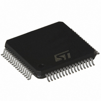
ST7FMC2R6T6 STMicroelectronics, ST7FMC2R6T6 Datasheet - Page 236

ST7FMC2R6T6
Manufacturer Part Number
ST7FMC2R6T6
Description
MCU 8BIT 32K FLASH 64TQFP
Manufacturer
STMicroelectronics
Series
ST7r
Datasheet
1.ST7FMC2S4T6.pdf
(309 pages)
Specifications of ST7FMC2R6T6
Core Processor
ST7
Core Size
8-Bit
Speed
8MHz
Connectivity
LINSCI, SPI
Peripherals
LVD, Motor Control PWM, POR, PWM, WDT
Number Of I /o
44
Program Memory Size
32KB (32K x 8)
Program Memory Type
FLASH
Ram Size
1K x 8
Voltage - Supply (vcc/vdd)
3.8 V ~ 5.5 V
Data Converters
A/D 16x10b
Oscillator Type
Internal
Operating Temperature
-40°C ~ 85°C
Package / Case
64-TQFP, 64-VQFP
Processor Series
ST7FMC2x
Core
ST7
Data Bus Width
8 bit
Data Ram Size
1 KB
Interface Type
SCI, SPI
Maximum Clock Frequency
8 MHz
Number Of Programmable I/os
60
Number Of Timers
3
Maximum Operating Temperature
+ 85 C
Mounting Style
SMD/SMT
Development Tools By Supplier
ST7MC-KIT/BLDC, ST7MDT50-EMU3, STX-RLINK
Minimum Operating Temperature
- 40 C
On-chip Adc
10 bit, 16 Channel
For Use With
497-8402 - BOARD EVAL COMPLETE INVERTER497-8400 - KIT IGBT PWR MODULE CTRL ST7MC497-6408 - BOARD EVAL BLDC SENSORLESS MOTOR497-4734 - EVAL KIT 3KW POWER DRIVER BOARD497-4733 - EVAL KIT 1KW POWER DRIVER BOARD497-4732 - EVAL KIT 300W POWER DRIVER BOARD497-4731 - EVAL KIT PWR DRIVER CONTROL BRD
Lead Free Status / RoHS Status
Lead free / RoHS Compliant
Eeprom Size
-
Lead Free Status / Rohs Status
Details
Other names
497-4868
Available stocks
Company
Part Number
Manufacturer
Quantity
Price
Company:
Part Number:
ST7FMC2R6T6
Manufacturer:
STMicroelectronics
Quantity:
10 000
- Current page: 236 of 309
- Download datasheet (6Mb)
ST7MC1xx/ST7MC2xx
10.8 10-BIT A/D CONVERTER (ADC)
10.8.1 Introduction
The on-chip Analog to Digital Converter (ADC) pe-
ripheral is a 10-bit, successive approximation con-
verter with internal sample and hold circuitry. This
peripheral has up to 16 multiplexed analog input
channels (refer to device pin out description) that
allow the peripheral to convert the analog voltage
levels from up to 16 different sources.
The result of the conversion is stored in 2 8-bit
Data Registers. The A/D converter is controlled
through a Control/Status Register.
10.8.2 Main Features
■
■
■
■
■
■
Figure 127. ADC Block Diagram
236/309
10-bit conversion
Up to 16 channels with multiplexed input
2 software-selectable sample times
External positive reference voltage V
be independent from supply
Linear successive approximation
Data registers (DR) which contain the results
AIN0
AINx
AIN1
f
ADC
ANALOG
MUX
EOC PRSC1PRSC0 ADON
PRESCALER
ADCDRMSB
MCCBCR
4
REF+
ADCDRLSB
CS3
D9
can
CS2
ADSTS
D8
■
■
■
The block diagram is shown in
10.8.3 Functional Description
10.8.3.1 Analog References
V
ence voltage pins. Conversion accuracy may
therefore be impacted by voltage drops and noise
on these lines. V
mediate supply between V
change the conversion voltage range. V
be tied to V
plemented between V
typical value of 15k
10.8.3.2 Analog Power Supply
V
providing power to the converter part. They must
be tied to V
CS1
D7
ADCIE
REF+
DDA
Conversion complete status flag
Maskable interrupt
On/off bit (to reduce consumption)
0
CS0
and V
D6
and V
0
D5
DD
ADCCSR
SSA
SSA
REF-
0
and V
. An internal resistor bridge is im-
request
D4
REF+
are the supply and ground pins
are the high and low level refer-
IT
0
ANALOG TO DIGITAL
Ω
SS
D3
can be supplied by an inter-
REF+
CONVERTER
respectively.
0
D2
and V
0
DDA
Figure
D1
REF-
and V
127.
D0
pins, with a
REF-
SSA
must
to
Related parts for ST7FMC2R6T6
Image
Part Number
Description
Manufacturer
Datasheet
Request
R

Part Number:
Description:
STMicroelectronics [RIPPLE-CARRY BINARY COUNTER/DIVIDERS]
Manufacturer:
STMicroelectronics
Datasheet:

Part Number:
Description:
STMicroelectronics [LIQUID-CRYSTAL DISPLAY DRIVERS]
Manufacturer:
STMicroelectronics
Datasheet:

Part Number:
Description:
BOARD EVAL FOR MEMS SENSORS
Manufacturer:
STMicroelectronics
Datasheet:

Part Number:
Description:
NPN TRANSISTOR POWER MODULE
Manufacturer:
STMicroelectronics
Datasheet:

Part Number:
Description:
TURBOSWITCH ULTRA-FAST HIGH VOLTAGE DIODE
Manufacturer:
STMicroelectronics
Datasheet:

Part Number:
Description:
Manufacturer:
STMicroelectronics
Datasheet:

Part Number:
Description:
DIODE / SCR MODULE
Manufacturer:
STMicroelectronics
Datasheet:

Part Number:
Description:
DIODE / SCR MODULE
Manufacturer:
STMicroelectronics
Datasheet:

Part Number:
Description:
Search -----> STE16N100
Manufacturer:
STMicroelectronics
Datasheet:

Part Number:
Description:
Search ---> STE53NA50
Manufacturer:
STMicroelectronics
Datasheet:

Part Number:
Description:
NPN Transistor Power Module
Manufacturer:
STMicroelectronics
Datasheet:

Part Number:
Description:
DIODE / SCR MODULE
Manufacturer:
STMicroelectronics
Datasheet:


