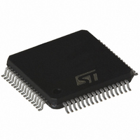
ST7FMC2R6T6 STMicroelectronics, ST7FMC2R6T6 Datasheet - Page 221

ST7FMC2R6T6
Manufacturer Part Number
ST7FMC2R6T6
Description
MCU 8BIT 32K FLASH 64TQFP
Manufacturer
STMicroelectronics
Series
ST7r
Datasheet
1.ST7FMC2S4T6.pdf
(309 pages)
Specifications of ST7FMC2R6T6
Core Processor
ST7
Core Size
8-Bit
Speed
8MHz
Connectivity
LINSCI, SPI
Peripherals
LVD, Motor Control PWM, POR, PWM, WDT
Number Of I /o
44
Program Memory Size
32KB (32K x 8)
Program Memory Type
FLASH
Ram Size
1K x 8
Voltage - Supply (vcc/vdd)
3.8 V ~ 5.5 V
Data Converters
A/D 16x10b
Oscillator Type
Internal
Operating Temperature
-40°C ~ 85°C
Package / Case
64-TQFP, 64-VQFP
Processor Series
ST7FMC2x
Core
ST7
Data Bus Width
8 bit
Data Ram Size
1 KB
Interface Type
SCI, SPI
Maximum Clock Frequency
8 MHz
Number Of Programmable I/os
60
Number Of Timers
3
Maximum Operating Temperature
+ 85 C
Mounting Style
SMD/SMT
Development Tools By Supplier
ST7MC-KIT/BLDC, ST7MDT50-EMU3, STX-RLINK
Minimum Operating Temperature
- 40 C
On-chip Adc
10 bit, 16 Channel
For Use With
497-8402 - BOARD EVAL COMPLETE INVERTER497-8400 - KIT IGBT PWR MODULE CTRL ST7MC497-6408 - BOARD EVAL BLDC SENSORLESS MOTOR497-4734 - EVAL KIT 3KW POWER DRIVER BOARD497-4733 - EVAL KIT 1KW POWER DRIVER BOARD497-4732 - EVAL KIT 300W POWER DRIVER BOARD497-4731 - EVAL KIT PWR DRIVER CONTROL BRD
Lead Free Status / RoHS Status
Lead free / RoHS Compliant
Eeprom Size
-
Lead Free Status / Rohs Status
Details
Other names
497-4868
Available stocks
Company
Part Number
Manufacturer
Quantity
Price
Company:
Part Number:
ST7FMC2R6T6
Manufacturer:
STMicroelectronics
Quantity:
10 000
- Current page: 221 of 309
- Download datasheet (6Mb)
MOTOR CONTROLLER (Cont’d)
DEAD TIME GENERATOR REGISTER (MDTG)
Read/Write (except bits 5:0 write once-only)
Reset Value: 1111 1111 (FFh)
Bit 7 = PCN: Number of PWM Channels .
0: Only PWM U signal is output to the PWM man-
1: The three PWM signals U, V and W are output
Bit 6 = DTE*: Dead Time Generator Enable
0: Disable the Dead Time generator
1: Enable the Dead Time generator and apply
* write once-only bit if PCN bit is set, read/write if
Table 74. DeadTime generator set-up
Note 1: This table is true on condition that the CKE
bit is set (Peripheral clock enabled) and the MOE
bit is set (MCOx outputs enabled). See Table 56,
“Output configuration summary,” on page 210
PCN
DAC
ager for six-step mode motor control (e.g. PM
BLDC motors)
to the channel manager (e.g. for three-phase
sinewave generation)
complementary PWM signal to the adjacent
switch
PCN bit is reset. To clear the DTE bit if PCN=1,
it is mandatory to clear the PCN bit first.
7
0
0
0
0
1
1
1
1
DTE
in MDTG
register
PCN bit
0
0
1
1
0
0
1
1
DTG5 DTG4 DTG3 DTG2
in MDTG
register
DTE bit
0
1
1
0
0
1
1
0
Complementary PWM
applied to adjacent
WITHOUT deadtime
WITHOUT deadtime
NO Complementary
YES, but
YES, but
switch
PWM
YES
YES
YES
YES
NO
DTG1
DTG0
0
When the PCN bit is reset (e.g. for PM BLDC mo-
tors), in Direct Access mode (DAC=1), if the DTE
bit is reset, PWM signals can be applied on the
MCOx outputs but not complementary PWM. Of
course, logical levels can be also applied on the
outputs.
If the DTE bit is set (PCN=0 and DAC=1), chan-
nels are paired and complementary PWM signals
can be output on the MCOx pins. This will follow
the rules detailed in Table 53, “Dead Time genera-
tor outputs,” on page 197 as the channels are
grouped in pairs.
In this case, the PWM application is selected by
the OS0 bit in the MCRB register.
It is also possible to add a chopper on the PWM
signal output using bits HFE[1:0] and HFRQ[2:0] in
the MREF register.
Caution 1: The PWM mode will be selected via
the 00[5:0] bits in the MPHST register, the OE[5:0]
bits in the MPAR register and the OS2 and OS0
bits in the MCRB register as shown in Table 62,
“PWM mode when SR=1,” on page 213.
Caution 2: When driving motors with three inde-
pendent pairs of complementary PWM signals
(PCN=1), disabling the deadtime generator
(DTE=0) causes the deadtime to be null: high and
low side signals are exactly complemented.
It is therefore recommended not to disable the
deadtime generator (it may damage the power
stage), unless deadtimes are inserted externally.
Bits 5:0 = DTG[5:0]* Dead time generator set-up.
These bits set-up the deadtime duration and reso-
lution. Refer to Table 52, “Dead time programming
and example,” on page 195 for details.
With
125ns to 16µs with steps of 125ns, 250ns and
500ns.
* Write-once bits; once write-accessed these bits
cannot be re-written unless the processor is reset
(See “Caution: Access to write-once bits” on
page 220.).
F
mtc
= 16MHz dead time values range from
ST7MC1xx/ST7MC2xx
221/309
Related parts for ST7FMC2R6T6
Image
Part Number
Description
Manufacturer
Datasheet
Request
R

Part Number:
Description:
STMicroelectronics [RIPPLE-CARRY BINARY COUNTER/DIVIDERS]
Manufacturer:
STMicroelectronics
Datasheet:

Part Number:
Description:
STMicroelectronics [LIQUID-CRYSTAL DISPLAY DRIVERS]
Manufacturer:
STMicroelectronics
Datasheet:

Part Number:
Description:
BOARD EVAL FOR MEMS SENSORS
Manufacturer:
STMicroelectronics
Datasheet:

Part Number:
Description:
NPN TRANSISTOR POWER MODULE
Manufacturer:
STMicroelectronics
Datasheet:

Part Number:
Description:
TURBOSWITCH ULTRA-FAST HIGH VOLTAGE DIODE
Manufacturer:
STMicroelectronics
Datasheet:

Part Number:
Description:
Manufacturer:
STMicroelectronics
Datasheet:

Part Number:
Description:
DIODE / SCR MODULE
Manufacturer:
STMicroelectronics
Datasheet:

Part Number:
Description:
DIODE / SCR MODULE
Manufacturer:
STMicroelectronics
Datasheet:

Part Number:
Description:
Search -----> STE16N100
Manufacturer:
STMicroelectronics
Datasheet:

Part Number:
Description:
Search ---> STE53NA50
Manufacturer:
STMicroelectronics
Datasheet:

Part Number:
Description:
NPN Transistor Power Module
Manufacturer:
STMicroelectronics
Datasheet:

Part Number:
Description:
DIODE / SCR MODULE
Manufacturer:
STMicroelectronics
Datasheet:


