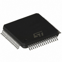
ST7FMC2R6T6 STMicroelectronics, ST7FMC2R6T6 Datasheet - Page 220

ST7FMC2R6T6
Manufacturer Part Number
ST7FMC2R6T6
Description
MCU 8BIT 32K FLASH 64TQFP
Manufacturer
STMicroelectronics
Series
ST7r
Datasheet
1.ST7FMC2S4T6.pdf
(309 pages)
Specifications of ST7FMC2R6T6
Core Processor
ST7
Core Size
8-Bit
Speed
8MHz
Connectivity
LINSCI, SPI
Peripherals
LVD, Motor Control PWM, POR, PWM, WDT
Number Of I /o
44
Program Memory Size
32KB (32K x 8)
Program Memory Type
FLASH
Ram Size
1K x 8
Voltage - Supply (vcc/vdd)
3.8 V ~ 5.5 V
Data Converters
A/D 16x10b
Oscillator Type
Internal
Operating Temperature
-40°C ~ 85°C
Package / Case
64-TQFP, 64-VQFP
Processor Series
ST7FMC2x
Core
ST7
Data Bus Width
8 bit
Data Ram Size
1 KB
Interface Type
SCI, SPI
Maximum Clock Frequency
8 MHz
Number Of Programmable I/os
60
Number Of Timers
3
Maximum Operating Temperature
+ 85 C
Mounting Style
SMD/SMT
Development Tools By Supplier
ST7MC-KIT/BLDC, ST7MDT50-EMU3, STX-RLINK
Minimum Operating Temperature
- 40 C
On-chip Adc
10 bit, 16 Channel
For Use With
497-8402 - BOARD EVAL COMPLETE INVERTER497-8400 - KIT IGBT PWR MODULE CTRL ST7MC497-6408 - BOARD EVAL BLDC SENSORLESS MOTOR497-4734 - EVAL KIT 3KW POWER DRIVER BOARD497-4733 - EVAL KIT 1KW POWER DRIVER BOARD497-4732 - EVAL KIT 300W POWER DRIVER BOARD497-4731 - EVAL KIT PWR DRIVER CONTROL BRD
Lead Free Status / RoHS Status
Lead free / RoHS Compliant
Eeprom Size
-
Lead Free Status / Rohs Status
Details
Other names
497-4868
Available stocks
Company
Part Number
Manufacturer
Quantity
Price
Company:
Part Number:
ST7FMC2R6T6
Manufacturer:
STMicroelectronics
Quantity:
10 000
- Current page: 220 of 309
- Download datasheet (6Mb)
ST7MC1xx/ST7MC2xx
MOTOR CONTROLLER (Cont’d)
COMPARE PHASE U PRELOAD REGISTER
HIGH (MCPUH)
Read/Write
Reset Value: 0000 0000 (00h)
Bits 7:0 = CPUH[7:0] Most Significant Byte of
phase U preload value
COMPARE PHASE U PRELOAD REGISTER
LOW (MCPUL)
Read/Write Read/Write (except bits 2:0)
Reset Value: 0000 0000 (00h)
Bits 7:5 = CPUL[7:3] Low bits of phase U preload
value.
Bits 2:0 = Reserved.
COMPARE 0 PRELOAD REGISTER HIGH
(MCP0H)
Read/Write (except bits 7:4)
Reset Value: 0000 1111 (0Fh)
Bits 7:4 = Reserved.
Bits 3:0 = CP0H[3:0] Most Significant Bits of Com-
pare 0 preload value.
220/309
CPUL7 CPUL6 CPUL5 CPUL4 CPUL3
CPUH
7
-
7
7
7
-
CPUH
6
-
CPUH
5
-
CPUH
CP0H3
4
CPUH
CP0H2
3
CPUH
2
-
CP0H1
CPUH
1
-
CP0H0
CPUH
0
0
0
0
-
COMPARE 0 PRELOAD REGISTER LOW
(MCP0L)
Read/Write
Reset Value: 1111 1111 (FFh)
Bits 7:0 = CP0L[7:0] Low byte of Compare 0
preload value.
Note 1: The 16-bit Compare registers MCMPOx,
MCMPUx, MCMPVx, MCMPWx MSB and LSB
parts have to be written sequentially before being
taken into account when an update event occurs;
refer to
Note 2: The CPB, HDM, SDM, OS2 bits in the
MCRB and the bits OE[5:0] are marked with *. It
means that these bits are taken into account at the
following commutation event (in normal mode) or
when a value is written in the MPHST register
when in direct access mode. For more details, re-
fer to the description of the DAC bit in the MCRA
register. The use of a Preload register allows all
the registers to be updated at the same time.
Warning: Access to Preload registers
Special care has to be taken with Preload regis-
ters, especially when using the ST7 BSET and
BRES instructions on MTC registers.
For instance, while writing to the MPHST register,
you will write the value in the preload register.
However, while reading at the same address, you
will get the current value in the register and not the
value of the preload register.
Excepted for three-phase PWM generator’s regis-
ters, all preload registers are loaded in the active
registers at the same time. In normal mode this is
done automatically when a C event occurs, how-
ever in direct access mode (DAC bit=1) the
preload registers are loaded as soon as a value is
written in the MPHST register.
Caution: Access to write-once bits
Special care has to be taken with write-once bits in
MPOL and MDTG registers; these bits have to be
accessed first during the set-up. Any access to the
other bits (not write-once) through a BRES or a
BSET instruction will lock the content of write-once
bits (no possibility for the core do distinguish indi-
vidual bit access: Read/write internal signal acts
on a whole register only). This protection is then
only unlocked after a processor hardware reset.
CP0L7 CP0L6 CP0L5 CP0L4 CP0L3 CP0L2 CP0L1 CP0L0
7
section 10.6.10.4 on page 201
for details.
0
Related parts for ST7FMC2R6T6
Image
Part Number
Description
Manufacturer
Datasheet
Request
R

Part Number:
Description:
STMicroelectronics [RIPPLE-CARRY BINARY COUNTER/DIVIDERS]
Manufacturer:
STMicroelectronics
Datasheet:

Part Number:
Description:
STMicroelectronics [LIQUID-CRYSTAL DISPLAY DRIVERS]
Manufacturer:
STMicroelectronics
Datasheet:

Part Number:
Description:
BOARD EVAL FOR MEMS SENSORS
Manufacturer:
STMicroelectronics
Datasheet:

Part Number:
Description:
NPN TRANSISTOR POWER MODULE
Manufacturer:
STMicroelectronics
Datasheet:

Part Number:
Description:
TURBOSWITCH ULTRA-FAST HIGH VOLTAGE DIODE
Manufacturer:
STMicroelectronics
Datasheet:

Part Number:
Description:
Manufacturer:
STMicroelectronics
Datasheet:

Part Number:
Description:
DIODE / SCR MODULE
Manufacturer:
STMicroelectronics
Datasheet:

Part Number:
Description:
DIODE / SCR MODULE
Manufacturer:
STMicroelectronics
Datasheet:

Part Number:
Description:
Search -----> STE16N100
Manufacturer:
STMicroelectronics
Datasheet:

Part Number:
Description:
Search ---> STE53NA50
Manufacturer:
STMicroelectronics
Datasheet:

Part Number:
Description:
NPN Transistor Power Module
Manufacturer:
STMicroelectronics
Datasheet:

Part Number:
Description:
DIODE / SCR MODULE
Manufacturer:
STMicroelectronics
Datasheet:


