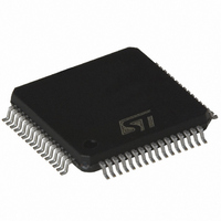
ST7FMC2R6T6 STMicroelectronics, ST7FMC2R6T6 Datasheet - Page 280

ST7FMC2R6T6
Manufacturer Part Number
ST7FMC2R6T6
Description
MCU 8BIT 32K FLASH 64TQFP
Manufacturer
STMicroelectronics
Series
ST7r
Datasheet
1.ST7FMC2S4T6.pdf
(309 pages)
Specifications of ST7FMC2R6T6
Core Processor
ST7
Core Size
8-Bit
Speed
8MHz
Connectivity
LINSCI, SPI
Peripherals
LVD, Motor Control PWM, POR, PWM, WDT
Number Of I /o
44
Program Memory Size
32KB (32K x 8)
Program Memory Type
FLASH
Ram Size
1K x 8
Voltage - Supply (vcc/vdd)
3.8 V ~ 5.5 V
Data Converters
A/D 16x10b
Oscillator Type
Internal
Operating Temperature
-40°C ~ 85°C
Package / Case
64-TQFP, 64-VQFP
Processor Series
ST7FMC2x
Core
ST7
Data Bus Width
8 bit
Data Ram Size
1 KB
Interface Type
SCI, SPI
Maximum Clock Frequency
8 MHz
Number Of Programmable I/os
60
Number Of Timers
3
Maximum Operating Temperature
+ 85 C
Mounting Style
SMD/SMT
Development Tools By Supplier
ST7MC-KIT/BLDC, ST7MDT50-EMU3, STX-RLINK
Minimum Operating Temperature
- 40 C
On-chip Adc
10 bit, 16 Channel
For Use With
497-8402 - BOARD EVAL COMPLETE INVERTER497-8400 - KIT IGBT PWR MODULE CTRL ST7MC497-6408 - BOARD EVAL BLDC SENSORLESS MOTOR497-4734 - EVAL KIT 3KW POWER DRIVER BOARD497-4733 - EVAL KIT 1KW POWER DRIVER BOARD497-4732 - EVAL KIT 300W POWER DRIVER BOARD497-4731 - EVAL KIT PWR DRIVER CONTROL BRD
Lead Free Status / RoHS Status
Lead free / RoHS Compliant
Eeprom Size
-
Lead Free Status / Rohs Status
Details
Other names
497-4868
Available stocks
Company
Part Number
Manufacturer
Quantity
Price
Company:
Part Number:
ST7FMC2R6T6
Manufacturer:
STMicroelectronics
Quantity:
10 000
- Current page: 280 of 309
- Download datasheet (6Mb)
ST7MC1xx/ST7MC2xx
12.13 OPERATIONAL AMPLIFIER CHARACTERISTICS
Subject to general operating conditions for f
(T
Note:
1. A
2. Data based on characterization results, not tested in production.
3. after offset compensation has been performed.
4. The amplifier accuracy is dependent on the environment. The offset value is given for a measurement done with all
digital I/Os stable. Negative injection current on the I/Os close to the inputs may reduce the accuracy. In particular care
must be taken to avoid switching on I/Os close to the inputs when the opamp is in use. This phenomenon is even more
critical when a big external serial resistor is added on the inputs.
5. The Data provided from simulations (not tested in production) to guide the user when re-calibration is needed.
6. The Data provided from simulations (not tested in production).
280/309
Symbol
V
V
T
V
SAT_OH
SAT_OL
CMR
A
wakeup
SVR
GBP
ΔV
SR
SR
A
Φm
CMIR
V
R
C
VCL
= -40..+125
vd
io
L
L
io
+
-
= closed loop gain
Resistive Load (max 500µA @
5V)
Capacitive Load at V
Common Mode Input Range
Input Offset Voltage ( + or - )
Input Offset Voltage Drift from
the calibrated Voltage, temper-
ature conditions
Common Mode Rejection
Ratio
Supply Voltage Rejection
Ratio
Voltage Gain
High Level Output Saturation
Voltage (V
Low Level Output Saturation
Voltage
Gain Bandwidth Product
Slew Rate while rising
Slew Rate while falling
Phase Margin
Wakeup time for the opamp
from off state
o
C, V
Parameter
DD
DD
-V
OUT
-V
SSA
)
OUT
= 4.5..5.5V unless otherwise specified
pin
3)
After calibration, V
with respect to temperature
with respect to common mode input
with respect to supply
HIGHGAIN=0 @ 100kHz
@ 100kHz
R
R
R
V
0dB gain, feedback resistor
ratio = 10 (20dB inverting con-
figuration)
HIGHGAIN=0
(A
2.75V)
HIGHGAIN=0
(A
2.75V)
HIGHGAIN=0
HIGHGAIN=1
OAP
L
L
L
VCL
VCL
=10kΩ
=10kΩ
=10kΩ
=1, R
=1, R
= V
OSC
1)
1)
DD
L
L
, and T
=10kΩ, C
=10kΩ, C
/ 2, measured at
Conditions
IC
A
=1V
L
L
unless otherwise specified.
=150pF, V
=150pF, V
HIGHGAIN=0
HIGHGAIN=1
i
i
=1.75V to
=1.75V to
(1.5)
1.3
2.6
0.8
V
2.5
Min Typ Max
50
1
10
SSA
2)
2)
2)
6)
2)
2)
2)
2.5 10
1.5
7.5
74
65
12
60
30
73
75
3
2
V
8.5
3.1
1.6
90
90
150
DD
1
2
4
5)
2)
2)
4)
2)
2)
/2
5)
5)
6)
degrees
μV/
mV/V
mV/V
V/mV
Unit
MHz
V/μs
V/μs
mV
mV
mV
kΩ
pF
dB
dB
μs
V
o
C
Related parts for ST7FMC2R6T6
Image
Part Number
Description
Manufacturer
Datasheet
Request
R

Part Number:
Description:
STMicroelectronics [RIPPLE-CARRY BINARY COUNTER/DIVIDERS]
Manufacturer:
STMicroelectronics
Datasheet:

Part Number:
Description:
STMicroelectronics [LIQUID-CRYSTAL DISPLAY DRIVERS]
Manufacturer:
STMicroelectronics
Datasheet:

Part Number:
Description:
BOARD EVAL FOR MEMS SENSORS
Manufacturer:
STMicroelectronics
Datasheet:

Part Number:
Description:
NPN TRANSISTOR POWER MODULE
Manufacturer:
STMicroelectronics
Datasheet:

Part Number:
Description:
TURBOSWITCH ULTRA-FAST HIGH VOLTAGE DIODE
Manufacturer:
STMicroelectronics
Datasheet:

Part Number:
Description:
Manufacturer:
STMicroelectronics
Datasheet:

Part Number:
Description:
DIODE / SCR MODULE
Manufacturer:
STMicroelectronics
Datasheet:

Part Number:
Description:
DIODE / SCR MODULE
Manufacturer:
STMicroelectronics
Datasheet:

Part Number:
Description:
Search -----> STE16N100
Manufacturer:
STMicroelectronics
Datasheet:

Part Number:
Description:
Search ---> STE53NA50
Manufacturer:
STMicroelectronics
Datasheet:

Part Number:
Description:
NPN Transistor Power Module
Manufacturer:
STMicroelectronics
Datasheet:

Part Number:
Description:
DIODE / SCR MODULE
Manufacturer:
STMicroelectronics
Datasheet:


