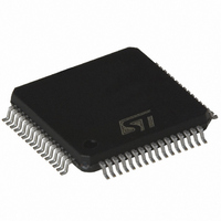
ST7FMC2R6T6 STMicroelectronics, ST7FMC2R6T6 Datasheet - Page 131

ST7FMC2R6T6
Manufacturer Part Number
ST7FMC2R6T6
Description
MCU 8BIT 32K FLASH 64TQFP
Manufacturer
STMicroelectronics
Series
ST7r
Datasheet
1.ST7FMC2S4T6.pdf
(309 pages)
Specifications of ST7FMC2R6T6
Core Processor
ST7
Core Size
8-Bit
Speed
8MHz
Connectivity
LINSCI, SPI
Peripherals
LVD, Motor Control PWM, POR, PWM, WDT
Number Of I /o
44
Program Memory Size
32KB (32K x 8)
Program Memory Type
FLASH
Ram Size
1K x 8
Voltage - Supply (vcc/vdd)
3.8 V ~ 5.5 V
Data Converters
A/D 16x10b
Oscillator Type
Internal
Operating Temperature
-40°C ~ 85°C
Package / Case
64-TQFP, 64-VQFP
Processor Series
ST7FMC2x
Core
ST7
Data Bus Width
8 bit
Data Ram Size
1 KB
Interface Type
SCI, SPI
Maximum Clock Frequency
8 MHz
Number Of Programmable I/os
60
Number Of Timers
3
Maximum Operating Temperature
+ 85 C
Mounting Style
SMD/SMT
Development Tools By Supplier
ST7MC-KIT/BLDC, ST7MDT50-EMU3, STX-RLINK
Minimum Operating Temperature
- 40 C
On-chip Adc
10 bit, 16 Channel
For Use With
497-8402 - BOARD EVAL COMPLETE INVERTER497-8400 - KIT IGBT PWR MODULE CTRL ST7MC497-6408 - BOARD EVAL BLDC SENSORLESS MOTOR497-4734 - EVAL KIT 3KW POWER DRIVER BOARD497-4733 - EVAL KIT 1KW POWER DRIVER BOARD497-4732 - EVAL KIT 300W POWER DRIVER BOARD497-4731 - EVAL KIT PWR DRIVER CONTROL BRD
Lead Free Status / RoHS Status
Lead free / RoHS Compliant
Eeprom Size
-
Lead Free Status / Rohs Status
Details
Other names
497-4868
Available stocks
Company
Part Number
Manufacturer
Quantity
Price
Company:
Part Number:
ST7FMC2R6T6
Manufacturer:
STMicroelectronics
Quantity:
10 000
- Current page: 131 of 309
- Download datasheet (6Mb)
LINSCI™ SERIAL COMMUNICATION INTERFACE (LIN Mode) (cont’d)
10.5.9.9 Error due to LIN Synch measurement
The LIN Synch Field is measured over eight bit
times.
This measurement is performed using a counter
clocked by the CPU clock. The edge detections
are performed using the CPU clock cycle.
This leads to a precision of 2 CPU clock cycles for
the measurement which lasts 16*8*LDIV clock cy-
cles.
Consequently, this error (D
2 / (128*LDIV
LDIV
er content, leading to the maximum baud rate, tak-
ing into account the maximum deviation of +/-15%.
10.5.9.10 Error due to Baud Rate Quantization
The baud rate can be adjusted in steps of 1 / (16 *
LDIV). The worst case occurs when the “real”
baud rate is in the middle of the step.
This leads to a quantization error (D
to 1 / (2*16*LDIV
10.5.9.11
Maximum Baud Rate
The choice of the nominal baud rate (LDIV
will influence both the quantization error (D
and the measurement error (D
case occurs for LDIV
MIN
corresponds to the minimum LIN prescal-
Impact
MIN
).
MIN
).
MIN
of
.
Clock
MEAS
MEAS
) is equal to:
Deviation
QUANT
). The worst
QUANT
) equal
NOM
on
)
)
Consequently, at a given CPU frequency, the
maximum possible nominal baud rate (LPR
should be chosen with respect to the maximum tol-
erated deviation given by the equation:
D
+ D
Example:
A nominal baud rate of 20Kbits/s at T
(8 MHz) leads to LDIV
LDIV
D
D
LIN Slave systems
For LIN Slave systems (the LINE and LSLV bits
are set), receivers wake up by LIN Synch Break or
LIN Identifier detection (depending on the LHDM
bit).
Hot Plugging Feature for LIN Slave Nodes
In LIN Slave Mute Mode (the LINE, LSLV and
RWU bits are set) it is possible to hot plug to a net-
work during an ongoing communication flow. In
this case the SCI monitors the bus on the RDI line
until 11 consecutive dominant bits have been de-
tected and discards all the other bits received.
TRA
MEAS
QUANT
REC
MIN
+ 2 / (128*LDIV
= 2 / (128*LDIV
+ D
= 1 / (2*16*LDIV
= 25 - 0.15*25 = 21.25
TCL
< 3.75%
MIN
NOM
MIN
ST7MC1xx/ST7MC2xx
) + 1 / (2*16*LDIV
MIN
) * 100 = 0.00073%
= 25d.
) * 100 = 0.0015%
CPU
= 125ns
MIN
131/309
MIN
)
1
)
Related parts for ST7FMC2R6T6
Image
Part Number
Description
Manufacturer
Datasheet
Request
R

Part Number:
Description:
STMicroelectronics [RIPPLE-CARRY BINARY COUNTER/DIVIDERS]
Manufacturer:
STMicroelectronics
Datasheet:

Part Number:
Description:
STMicroelectronics [LIQUID-CRYSTAL DISPLAY DRIVERS]
Manufacturer:
STMicroelectronics
Datasheet:

Part Number:
Description:
BOARD EVAL FOR MEMS SENSORS
Manufacturer:
STMicroelectronics
Datasheet:

Part Number:
Description:
NPN TRANSISTOR POWER MODULE
Manufacturer:
STMicroelectronics
Datasheet:

Part Number:
Description:
TURBOSWITCH ULTRA-FAST HIGH VOLTAGE DIODE
Manufacturer:
STMicroelectronics
Datasheet:

Part Number:
Description:
Manufacturer:
STMicroelectronics
Datasheet:

Part Number:
Description:
DIODE / SCR MODULE
Manufacturer:
STMicroelectronics
Datasheet:

Part Number:
Description:
DIODE / SCR MODULE
Manufacturer:
STMicroelectronics
Datasheet:

Part Number:
Description:
Search -----> STE16N100
Manufacturer:
STMicroelectronics
Datasheet:

Part Number:
Description:
Search ---> STE53NA50
Manufacturer:
STMicroelectronics
Datasheet:

Part Number:
Description:
NPN Transistor Power Module
Manufacturer:
STMicroelectronics
Datasheet:

Part Number:
Description:
DIODE / SCR MODULE
Manufacturer:
STMicroelectronics
Datasheet:


