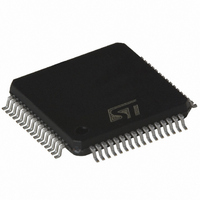
ST7FMC2R6T6 STMicroelectronics, ST7FMC2R6T6 Datasheet - Page 35

ST7FMC2R6T6
Manufacturer Part Number
ST7FMC2R6T6
Description
MCU 8BIT 32K FLASH 64TQFP
Manufacturer
STMicroelectronics
Series
ST7r
Datasheet
1.ST7FMC2S4T6.pdf
(309 pages)
Specifications of ST7FMC2R6T6
Core Processor
ST7
Core Size
8-Bit
Speed
8MHz
Connectivity
LINSCI, SPI
Peripherals
LVD, Motor Control PWM, POR, PWM, WDT
Number Of I /o
44
Program Memory Size
32KB (32K x 8)
Program Memory Type
FLASH
Ram Size
1K x 8
Voltage - Supply (vcc/vdd)
3.8 V ~ 5.5 V
Data Converters
A/D 16x10b
Oscillator Type
Internal
Operating Temperature
-40°C ~ 85°C
Package / Case
64-TQFP, 64-VQFP
Processor Series
ST7FMC2x
Core
ST7
Data Bus Width
8 bit
Data Ram Size
1 KB
Interface Type
SCI, SPI
Maximum Clock Frequency
8 MHz
Number Of Programmable I/os
60
Number Of Timers
3
Maximum Operating Temperature
+ 85 C
Mounting Style
SMD/SMT
Development Tools By Supplier
ST7MC-KIT/BLDC, ST7MDT50-EMU3, STX-RLINK
Minimum Operating Temperature
- 40 C
On-chip Adc
10 bit, 16 Channel
For Use With
497-8402 - BOARD EVAL COMPLETE INVERTER497-8400 - KIT IGBT PWR MODULE CTRL ST7MC497-6408 - BOARD EVAL BLDC SENSORLESS MOTOR497-4734 - EVAL KIT 3KW POWER DRIVER BOARD497-4733 - EVAL KIT 1KW POWER DRIVER BOARD497-4732 - EVAL KIT 300W POWER DRIVER BOARD497-4731 - EVAL KIT PWR DRIVER CONTROL BRD
Lead Free Status / RoHS Status
Lead free / RoHS Compliant
Eeprom Size
-
Lead Free Status / Rohs Status
Details
Other names
497-4868
Available stocks
Company
Part Number
Manufacturer
Quantity
Price
Company:
Part Number:
ST7FMC2R6T6
Manufacturer:
STMicroelectronics
Quantity:
10 000
- Current page: 35 of 309
- Download datasheet (6Mb)
SYSTEM INTEGRITY MANAGEMENT (Cont’d)
6.3.5 Register Description
SYSTEM INTEGRITY (SI) CONTROL/STATUS REGISTER (SICSR, page 0)
Read/Write
Reset Value: 000x 000x (00h)
Bit 7 = PAGE SICSR Register Page Selection
This bit selects the SICSR register page. It is set
and cleared by software
0: Access to SICSR register mapped in page 0.
1: Access to SICSR register mapped in page 1.
Bit 6 = AVDIE Voltage Detector interrupt enable
This bit is set and cleared by software. It enables
an interrupt to be generated when the AVDF flag
changes (toggles). The pending interrupt informa-
tion is automatically cleared when software enters
the AVD interrupt routine.
0: AVD interrupt disabled
1: AVD interrupt enabled
Bit 5 = AVDF Voltage Detector flag
This read-only bit is set and cleared by hardware.
If the VDIE bit is set, an interrupt request is gener-
ated when the AVDF bit changes value.
0: V
1: V
Bit 4 = LVDRF LVD reset flag
This bit indicates that the last Reset was generat-
ed by the LVD block. It is set by hardware (LVD re-
set) and cleared by software (writing zero). See
WDGRF flag description for more details. When
the LVD is disabled by OPTION BYTE, the LVDRF
bit value is undefined.
Bit 3 = Reserved, must be kept cleared.
Bit 2 = CSSIE Clock security syst
This bit enables the interrupt when a disturbance
PAG
E
7
DD
DD
under V
over V
AVD
IE
AVD
IT+ (AVD)
F
IT-(AVD)
LVD
RF
threshold
threshold
0
CSS
.
IE
interrupt enable
CSS
D
WDG
RF
0
is detected by the Clock Security System (CSSD
bit set). It is set and cleared by software.
0: Clock security system interrupt disabled
1: Clock security system interrupt enabled
When the PLL is disabled (PLLEN=0), the CSSIE
bit has no effect.
Bit 1 = CSSD Clock security system detection
This bit indicates a disturbance on the main clock
signal (f
cles). It is set by hardware and cleared by reading
the SICSR register when the original oscillator re-
covers.
0: Safe oscillator is not active
1: Safe oscillator has been activated
When the PLL is disabled (PLLEN=0), the CSSD
bit value is forced to 0.
Bit 0 = WDGRF Watchdog reset flag
This bit indicates that the last Reset was generat-
ed by the Watchdog peripheral. It is set by hard-
ware (watchdog reset) and cleared by software
(writing zero) or an LVD Reset (to ensure a stable
cleared state of the WDGRF flag when CPU
starts).
Combined with the LVDRF flag information, the
flag description is given by the following table.
Application notes
The LVDRF flag is not cleared when another RE-
SET type occurs (external or watchdog), the
LVDRF flag remains set to keep trace of the origi-
nal failure.
In this case, a watchdog reset can be detected by
software while an external reset can not.
External RESET pin
OSC
RESET Sources
Watchdog
): the clock stops (at least for a few cy-
LVD
ST7MC1xx/ST7MC2xx
LVDRF
0
0
1
WDGRF
35/309
X
0
1
1
Related parts for ST7FMC2R6T6
Image
Part Number
Description
Manufacturer
Datasheet
Request
R

Part Number:
Description:
STMicroelectronics [RIPPLE-CARRY BINARY COUNTER/DIVIDERS]
Manufacturer:
STMicroelectronics
Datasheet:

Part Number:
Description:
STMicroelectronics [LIQUID-CRYSTAL DISPLAY DRIVERS]
Manufacturer:
STMicroelectronics
Datasheet:

Part Number:
Description:
BOARD EVAL FOR MEMS SENSORS
Manufacturer:
STMicroelectronics
Datasheet:

Part Number:
Description:
NPN TRANSISTOR POWER MODULE
Manufacturer:
STMicroelectronics
Datasheet:

Part Number:
Description:
TURBOSWITCH ULTRA-FAST HIGH VOLTAGE DIODE
Manufacturer:
STMicroelectronics
Datasheet:

Part Number:
Description:
Manufacturer:
STMicroelectronics
Datasheet:

Part Number:
Description:
DIODE / SCR MODULE
Manufacturer:
STMicroelectronics
Datasheet:

Part Number:
Description:
DIODE / SCR MODULE
Manufacturer:
STMicroelectronics
Datasheet:

Part Number:
Description:
Search -----> STE16N100
Manufacturer:
STMicroelectronics
Datasheet:

Part Number:
Description:
Search ---> STE53NA50
Manufacturer:
STMicroelectronics
Datasheet:

Part Number:
Description:
NPN Transistor Power Module
Manufacturer:
STMicroelectronics
Datasheet:

Part Number:
Description:
DIODE / SCR MODULE
Manufacturer:
STMicroelectronics
Datasheet:


