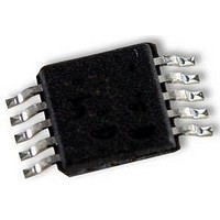
UPD78F9502MA-CAC-A NEC, UPD78F9502MA-CAC-A Datasheet - Page 140

UPD78F9502MA-CAC-A
Manufacturer Part Number
UPD78F9502MA-CAC-A
Description
8BIT MCU, 4K FLASH, 128B RAM, SMD
Manufacturer
NEC
Datasheet
1.UPD78F9502MA-CAC-A.pdf
(229 pages)
Specifications of UPD78F9502MA-CAC-A
Controller Family/series
UPD78F
No. Of I/o's
8
Ram Memory Size
128Byte
Cpu Speed
10MHz
No. Of Timers
2
No. Of Pwm
RoHS Compliant
Core Size
8bit
Program Memory Size
4KB
Oscillator Type
External, Internal
- Current page: 140 of 229
- Download datasheet (2Mb)
14.6
provided on the target system. First provide a function that selects the normal operation mode or flash memory
programming mode on the board.
the same status as immediately after reset. Therefore, if the external device does not recognize the state immediately
after reset, the pins must be processed as described below.
14.6.1 EXCLK pin
connected to an external device, a signal conflict occurs. To prevent the conflict of signals, isolate the connection with
the external device.
there is a possibility that cannot communicate depending on capacitor capacitance. When perform flash memory
programming, isolate connection with a condenser.
140
Note In the PD78F9500, 78F9501, 78F9502, the CLK and FLMD0 signals are connected to the EXCLK pin;
To write the flash memory on-board, connectors that connect the dedicated flash memory programmer must be
When the flash memory programming mode is set, all the pins not used for programming the flash memory are in
The state of the pins in the self programming mode is the same as that in the HALT mode.
The EXCLK pin is used as the serial interface of flash memory programming. Therefore, if the EXCLK pin is
When connected a capacitor to the EXCLK pin, waveform at the time of communication is changed. Therefore
CLK
FLMD0
SI/RxD
SO/TxD
/RESET
V
GND
Pin Name
Processing of Pins on Board
DD
Note
therefore, these signals need to be directly connected.
Note
Note
Note
Table 14-2. Wiring Between PD78F9500, 78F9501, 78F9502, and FlashPro4
Output
Output
Input
Output
Output
I/O
–
–
FlashPro4 Connection Pin
Clock to PD78F9500, 78F9501, 78F9502
On-board mode signal
Receive signal
Receive signal/on-board mode signal
Reset signal
V
Ground
DD
Figure 14-3. Wiring diagram with FlashPro4
/RESET
signal name
SO/TxD
FLMD0
SI/RxD
FlashPro4
voltage generation/voltage monitor
GND
CLK
V
DD
Preliminary User’s Manual U18681EJ1V0UD
CHAPTER 14 FLASH MEMORY
Pin Function
78F9501, 78F9502
1
2
3
4
5
PD78F9500,
EXCLK/P23
P22
RESET/P34
V
V
10
9
8
7
6
DD
SS
PD78F9500, 78F9501, 78F9502
Pin Name
Connection Pin
5
6
7
4
3
Pin No.
Related parts for UPD78F9502MA-CAC-A
Image
Part Number
Description
Manufacturer
Datasheet
Request
R

Part Number:
Description:
16/8 bit single-chip microcomputer
Manufacturer:
NEC
Datasheet:

Part Number:
Description:
Dual audio power amp circuit
Manufacturer:
NEC
Datasheet:

Part Number:
Description:
Dual comparator
Manufacturer:
NEC
Datasheet:

Part Number:
Description:
MOS type composite field effect transistor
Manufacturer:
NEC
Datasheet:

Part Number:
Description:
50 V/100 mA FET array incorporating 2 N-ch MOSFETs
Manufacturer:
NEC
Datasheet:

Part Number:
Description:
6-pin small MM high-frequency double transistor
Manufacturer:
NEC
Datasheet:

Part Number:
Description:
6-pin small MM high-frequency double transistor
Manufacturer:
NEC
Datasheet:

Part Number:
Description:
6-pin small MM high-frequency double transistor
Manufacturer:
NEC
Datasheet:

Part Number:
Description:
6-pin small MM high-frequency double transistor
Manufacturer:
NEC
Datasheet:

Part Number:
Description:
Twin transistors equipped with different model chips(6P small MM)
Manufacturer:
NEC
Datasheet:

Part Number:
Description:
Bipolar analog integrated circuit
Manufacturer:
NEC
Datasheet:


