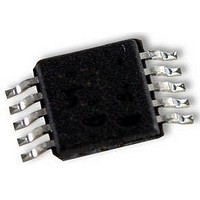
UPD78F9502MA-CAC-A NEC, UPD78F9502MA-CAC-A Datasheet - Page 63

UPD78F9502MA-CAC-A
Manufacturer Part Number
UPD78F9502MA-CAC-A
Description
8BIT MCU, 4K FLASH, 128B RAM, SMD
Manufacturer
NEC
Datasheet
1.UPD78F9502MA-CAC-A.pdf
(229 pages)
Specifications of UPD78F9502MA-CAC-A
Controller Family/series
UPD78F
No. Of I/o's
8
Ram Memory Size
128Byte
Cpu Speed
10MHz
No. Of Timers
2
No. Of Pwm
RoHS Compliant
Core Size
8bit
Program Memory Size
4KB
Oscillator Type
External, Internal
- Current page: 63 of 229
- Download datasheet (2Mb)
5.3
The clock generators are controlled by the following three registers.
(1) Processor clock control register (PCC) and preprocessor clock control register (PPCC)
Address: FFFBH, After reset: 02H, R/W
Symbol
PCC
Address: FFF3H, After reset: 02H, R/W
Symbol
PPCC
Processor clock control register (PCC)
Preprocessor clock control register (PPCC)
Low-speed internal oscillation mode register (LSRCM)
Registers Controlling Clock Generators
These registers are used to specify the division ratio of the system clock.
PCC and PPCC are set by using a 1-bit or 8-bit memory manipulation instruction.
Reset signal generation sets PCC and PPCC to 02H.
Notes 1.
PPCC1
7
0
7
0
0
0
0
1
0
1
Figure 5-3. Format of Preprocessor Clock Control Register (PPCC)
2. If PPCC = 01H, the clock (f
3. If PPCC = 02H, the clock (f
Figure 5-2. Format of Processor Clock Control Register (PCC)
Other than above
The setting range of the CPU clock differs depending on the supply voltage to be used.
Be sure to refer to CPU clock and peripheral clock frequencies described in AC
Characteristics in CHAPTER 16 ELECTRICAL SPECIFICATIONS (TARGET).
PPCC0
6
0
6
0
0
1
0
0
1
0
CHAPTER 5 CLOCK GENERATORS
Preliminary User’s Manual U18681EJ1V0UD
PCC1
5
0
5
0
0
0
1
0
1
1
f
f
f
f
f
f
Setting prohibited
X
X
X
X
X
X
/2
/2
/2
/2
/2
XP
XP
2
2 Note 3
3 Note 2
4 Note 3
Note 2
) supplied to the peripheral hardware is f
) supplied to the peripheral hardware is f
4
0
4
0
Selection of CPU clock (f
3
0
3
0
2
0
2
0
CPU
PPCC1
PCC1
)
1
1
Note 1
X
X
/2.
/2
2
.
PPCC0
0
0
0
63
Related parts for UPD78F9502MA-CAC-A
Image
Part Number
Description
Manufacturer
Datasheet
Request
R

Part Number:
Description:
16/8 bit single-chip microcomputer
Manufacturer:
NEC
Datasheet:

Part Number:
Description:
Dual audio power amp circuit
Manufacturer:
NEC
Datasheet:

Part Number:
Description:
Dual comparator
Manufacturer:
NEC
Datasheet:

Part Number:
Description:
MOS type composite field effect transistor
Manufacturer:
NEC
Datasheet:

Part Number:
Description:
50 V/100 mA FET array incorporating 2 N-ch MOSFETs
Manufacturer:
NEC
Datasheet:

Part Number:
Description:
6-pin small MM high-frequency double transistor
Manufacturer:
NEC
Datasheet:

Part Number:
Description:
6-pin small MM high-frequency double transistor
Manufacturer:
NEC
Datasheet:

Part Number:
Description:
6-pin small MM high-frequency double transistor
Manufacturer:
NEC
Datasheet:

Part Number:
Description:
6-pin small MM high-frequency double transistor
Manufacturer:
NEC
Datasheet:

Part Number:
Description:
Twin transistors equipped with different model chips(6P small MM)
Manufacturer:
NEC
Datasheet:

Part Number:
Description:
Bipolar analog integrated circuit
Manufacturer:
NEC
Datasheet:


