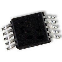
UPD78F9502MA-CAC-A NEC, UPD78F9502MA-CAC-A Datasheet - Page 166

UPD78F9502MA-CAC-A
Manufacturer Part Number
UPD78F9502MA-CAC-A
Description
8BIT MCU, 4K FLASH, 128B RAM, SMD
Manufacturer
NEC
Datasheet
1.UPD78F9502MA-CAC-A.pdf
(229 pages)
Specifications of UPD78F9502MA-CAC-A
Controller Family/series
UPD78F
No. Of I/o's
8
Ram Memory Size
128Byte
Cpu Speed
10MHz
No. Of Timers
2
No. Of Pwm
RoHS Compliant
Core Size
8bit
Program Memory Size
4KB
Oscillator Type
External, Internal
- Current page: 166 of 229
- Download datasheet (2Mb)
14.8.8 Example of byte write operation in self programming mode
166
An example of the byte write operation in self programming mode is explained below.
<1> Set 05H (byte write) to the flash program command register (FLCMD).
<2> Set the number of block to which data is to be written, to flash address pointer H (FLAPH).
<3> Set the address at which data is to be written, to flash address pointer L (FLAPL).
<4> Set the data to be written, to the flash write buffer register (FLW).
<5> Clear the flash status register (PFS).
<6> Write ACH to the watchdog timer enable register (WDTE) (clear and restart the watchdog timer counter)
<8> Check if a self programming error has occurred using bit 1 (VCERR) and bit 2 (WEPRERR) of PFS.
<9> Byte write processing is abnormally terminated.
<10> Byte write processing is normally terminated.
Note This setting is not required when the watchdog timer is not used.
Caution If a write results in failure, erase the block once and write to it again.
<7> Execute the HALT instruction then start self programming. (Execute an instruction immediately after the
Abnormal
Normal
HALT instruction if self programming has been executed.)
<9>
<10>
Preliminary User’s Manual U18681EJ1V0UD
CHAPTER 14 FLASH MEMORY
Note
.
Related parts for UPD78F9502MA-CAC-A
Image
Part Number
Description
Manufacturer
Datasheet
Request
R

Part Number:
Description:
16/8 bit single-chip microcomputer
Manufacturer:
NEC
Datasheet:

Part Number:
Description:
Dual audio power amp circuit
Manufacturer:
NEC
Datasheet:

Part Number:
Description:
Dual comparator
Manufacturer:
NEC
Datasheet:

Part Number:
Description:
MOS type composite field effect transistor
Manufacturer:
NEC
Datasheet:

Part Number:
Description:
50 V/100 mA FET array incorporating 2 N-ch MOSFETs
Manufacturer:
NEC
Datasheet:

Part Number:
Description:
6-pin small MM high-frequency double transistor
Manufacturer:
NEC
Datasheet:

Part Number:
Description:
6-pin small MM high-frequency double transistor
Manufacturer:
NEC
Datasheet:

Part Number:
Description:
6-pin small MM high-frequency double transistor
Manufacturer:
NEC
Datasheet:

Part Number:
Description:
6-pin small MM high-frequency double transistor
Manufacturer:
NEC
Datasheet:

Part Number:
Description:
Twin transistors equipped with different model chips(6P small MM)
Manufacturer:
NEC
Datasheet:

Part Number:
Description:
Bipolar analog integrated circuit
Manufacturer:
NEC
Datasheet:


