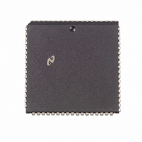
NS32FX164AV-25 National Semiconductor, NS32FX164AV-25 Datasheet - Page 58

NS32FX164AV-25
Manufacturer Part Number
NS32FX164AV-25
Description
IC IMAGING COMM SGNL PROC PLCC68
Manufacturer
National Semiconductor
Datasheet
1.NS32FX164AV-25.pdf
(102 pages)
Specifications of NS32FX164AV-25
Processor Type
Advanced Imaging/Communications Signal Processor SIAP™
Speed
50MHz
Voltage
5V
Mounting Type
Surface Mount
Package / Case
68-PLCC
Lead Free Status / RoHS Status
Contains lead / RoHS non-compliant
Features
-
Other names
*NS32FX164AV-25
Q1284286
Q1284286
Available stocks
Company
Part Number
Manufacturer
Quantity
Price
Company:
Part Number:
NS32FX164AV-25
Manufacturer:
NSC
Quantity:
12 388
Company:
Part Number:
NS32FX164AV-25
Manufacturer:
Texas Instruments
Quantity:
10 000
3 0 Functional Description
In general a SETCFG instruction must be executed in the
reset routine in order to properly configure the CPU The
options should be combined and executed in a single in-
struction For example to declare vectored interrupts a
Floating-Point unit installed and full CPU clock rate exe-
cute a SETCFG F I instruction To declare non-vectored
interrupts no FPU and full CPU clock rate execute a
SETCFG
3 5 5 Bus Cycles
The NS32FX164 will perform bus cycles for one of the fol-
lowing reasons
1 To fetch instructions from memory
2 To write or read data to or from memory or external pe-
3 To acknowledge an interrupt or to acknowledge comple-
4 To notify external logic of any accesses to the on-chip
5 To transfer information to or from a Slave Processor
3 5 5 1 Bus Status
The NS32FX164 CPU presents four bits of Bus Status infor-
mation on pins ST0–ST3 The various combinations on
these pins indicate why the CPU is performing a bus cycle
or if it is idle on the bus they why it is idle
The Bus Status pins are interpreted as a 4-bit value with
ST0 the least significant bit Their values decode as follows
0000
0001
0010
0011
0100
0101
0110
0111
1000
ripheral devices
tion of an interrupt service routine
peripheral device registers or internal RAM
The bus is idle because the CPU does not need to
perform a bus access
The bus is idle because the CPU is executing the
WAIT instruction
DSP Module Data Transfer
The bus is idle because the CPU is waiting for a
Slave Processor to complete an instruction
Interrupt Acknowledge Master
The CPU is performing a Read cycle to acknowl-
edge an interrupt request See Section 3 2 3
Interrupt Acknowledge Cascaded
The CPU is reading an interrupt vector to acknowl-
edge a maskable interrupt request from a Cascad-
ed Interrupt Control Unit
End of Interrupt Master
The CPU is performing a Read cycle to indicate
that it is executing a Return from Interrupt (RETI)
instruction at the completion of an interrupt’s serv-
ice procedure
End of Interrupt Cascaded
The CPU is performing a read cycle from a Cas-
caded Interrupt Control Unit to indicate that it is
executing a Return from Interrupt (RETI) instruc-
tion at the completion of an interrupt’s service pro-
cedure
Sequential Instruction Fetch
The CPU is reading the next sequential word from
the instruction stream into the Instruction Queue It
will do so whenever the bus would otherwise be
idle and the queue is not already full
instruction
(Continued)
58
1001
1010
1011
1100
1101
1110
1111
3 5 5 2 Basic Read and Write Cycles
The sequence of events occurring during a CPU access to
either memory or peripheral device is shown in Figure 3-21
for a read cycle and Figure 3-22 for a write cycle
The cases shown assume that the selected memory or pe-
ripheral device is capable of communicating with the CPU at
full speed If not then cycle extension may be requested
through CWAIT
A full-speed bus cycle is performed in four cycles of the
CTTL clock signal labeled T1 through T4 Clock cycles not
associated with a bus cycle are designated Ti (for ‘‘idle’’)
During T1 the CPU applies an address on pins AD0– AD15
and A16– A23 and provides a low-going pulse on the ADS
pin which serves the dual purpose of informing external
circuitry that a bus cycle is starting and of providing control
to an external latch for demultiplexing Address bits 0– 15
from the AD0 – AD15 pins It also deasserts the ALE signal
which eliminates the need to invert ADS to generate the
strobe for the address latches See Figure 3-20 During this
time also the status signals DDIN indicating the direction of
the transfer and HBE indicating whether the high byte
(AD8– AD15) is to be referenced become valid
During T2 the CPU switches the Data Bus AD0– AD15 to
either accept or present data Note that the signals A16–
A23 remain valid and need not be latched
Non-Sequential Instruction Fetch
The CPU is performing the first fetch of instruction
code after the Instruction Queue is purged This
will occur as a result of any jump or branch any
interrupt or trap or execution of certain instruc-
tions
Data Transfer
The CPU is reading or writing an operand of an
instruction
Read RMW Operand
The CPU is reading an operand which will subse-
quently be modified and rewritten The write cycle
of RMW will have a ‘‘write’’ status
Read for Effective Address Calculation
The CPU is reading information from memory in
order to determine the Effective Address of an op-
erand This will occur whenever an instruction uses
the Memory Relative or External addressing mode
Transfer Slave Processor Operand
The CPU is either transferring an instruction oper-
and to or from a Slave Processor or it is issuing
the Operation Word of a Slave Processor instruc-
tion
Read Slave Processor Status
The CPU is reading a Status Word from a Slave
Processor after the Slave Processor has signalled
completion of an instruction
Broadcast Slave ID
The CPU is initiating the execution of a Slave Proc-
essor instruction by transferring the first byte of the
instruction which represents the slave processor
indentification


