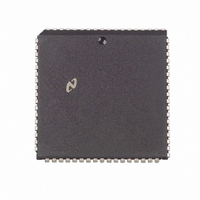
NS32FX164AV-25 National Semiconductor, NS32FX164AV-25 Datasheet - Page 74

NS32FX164AV-25
Manufacturer Part Number
NS32FX164AV-25
Description
IC IMAGING COMM SGNL PROC PLCC68
Manufacturer
National Semiconductor
Datasheet
1.NS32FX164AV-25.pdf
(102 pages)
Specifications of NS32FX164AV-25
Processor Type
Advanced Imaging/Communications Signal Processor SIAP™
Speed
50MHz
Voltage
5V
Mounting Type
Surface Mount
Package / Case
68-PLCC
Lead Free Status / RoHS Status
Contains lead / RoHS non-compliant
Features
-
Other names
*NS32FX164AV-25
Q1284286
Q1284286
Available stocks
Company
Part Number
Manufacturer
Quantity
Price
Company:
Part Number:
NS32FX164AV-25
Manufacturer:
NSC
Quantity:
12 388
Company:
Part Number:
NS32FX164AV-25
Manufacturer:
Texas Instruments
Quantity:
10 000
Symbol
V
V
V
V
V
V
V
V
V
V
I
I
I
I
ILS
I
L
CC
IH
IL
XL
XH
RIH
RIL
RHYS
HYS
OH
OL
4 0 Device Specifications
4 2 ABSOLUTE MAXIMUM RATINGS
If Military Aerospace specified devices are required
please contact the National Semiconductor Sales
Office Distributors for availability and specifications
Temperature under Bias
Storage Temperature
4 3 ELECTRICAL CHARACTERISTICS T
Note 1 Care should be taken by designers to provide a minimum inductance path between the GND pins and system ground in order to minimize noise
Note 2 I
4 4 SWITCHING CHARACTERISTICS
4 4 1 Definitions
All the timing specifications given in this section refer to
0 8V or 2 0V on the rising or falling edges of all the signals
as illustrated in Figures 4-2 and 4-3 unless specifically stat-
ed otherwise The capacitive load is assumed to be 100 pF
on CTTL and 50 pF on all the other output signals
FIGURE 4-2 Output Signals Specification Standard
CC
High Level Input Voltage
Low Level Input Voltage
OSCIN Input Low Voltage
OSCIN Input High Voltage
RSTI High Level Input Voltage
RSTI Low Level Input Voltage
RSTI Hysteresis Loop Width (Note 3)
INT NMI Hysteresis Loop Width (Note 3)
High Level Output Voltage
Low Level Output Voltage
SPC Input Current (Low)
Input Load Current
Leakage Current
Output and I O Pins in
TRI-STATE or Input Mode
Active Supply Current
is affected by the clock scaling factor selected by the C- and M-bits in the CFG register see Section 3 5 3
Parameter
b
A
(Continued)
65 C to
e
0 C to
0 C to
TL EE 11267– 44
a
I
I
V
0
All Inputs except SPC
0 4
I
(Note 2)
OH
OL
OUT
a
IN
a
s
150 C
70 C
e
s
70 C V
e b
e
V
e
IN s
V
4 mA
0 4V SPC in Input Mode
OUT s
0 T
400 A
Conditions
74
V
CC
A
CC
e
e
V
which permanent damage may occur Continuous operation
at these limits is not intended operation should be limited to
those conditions specified under Electrical Characteristics
All Input or Output Voltages
Note Absolute maximum ratings indicate limits beyond
Abbreviations
L E
T E
CC
25 C
5V
with Respect to GND
FIGURE 4-3a Input Signals Specification Standard
g
Leading Edge
Traling Edge
10% GND
FIGURE 4-3b RSTI INT NMI Hysteresis
(3 5 V
e
0V
b
b
b
b
Max
Min
CC
2 0
3 8
0 5
0 2
2 4
0 5
0 5
20
20
b
1 5)
R E
F E
Typ
200
Falling Edge
Rising Edge
b
V
V
CC
CC
0 5V to
Max
0 45
0 8
0 5
0 7
1 0
TL EE 11267 – 45
TL EE 11267 – 71
20
20
a
a
0 5
0 5
a
6 5V
Units
mA
mA
V
V
V
V
V
V
V
V
V
V
A
A


