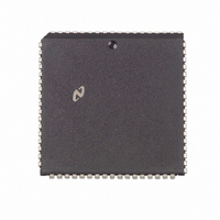
NS32FX164AV-25 National Semiconductor, NS32FX164AV-25 Datasheet - Page 67

NS32FX164AV-25
Manufacturer Part Number
NS32FX164AV-25
Description
IC IMAGING COMM SGNL PROC PLCC68
Manufacturer
National Semiconductor
Datasheet
1.NS32FX164AV-25.pdf
(102 pages)
Specifications of NS32FX164AV-25
Processor Type
Advanced Imaging/Communications Signal Processor SIAP™
Speed
50MHz
Voltage
5V
Mounting Type
Surface Mount
Package / Case
68-PLCC
Lead Free Status / RoHS Status
Contains lead / RoHS non-compliant
Features
-
Other names
*NS32FX164AV-25
Q1284286
Q1284286
Available stocks
Company
Part Number
Manufacturer
Quantity
Price
Company:
Part Number:
NS32FX164AV-25
Manufacturer:
NSC
Quantity:
12 388
Company:
Part Number:
NS32FX164AV-25
Manufacturer:
Texas Instruments
Quantity:
10 000
3-28
3 0 Functional Description
3 5 5 8 Data Access Sequences
The 24-bit address provided by the NS32FX164 is a byte
address
16 777 216 8-bit memory locations An important feature of
the NS32FX164 is that the presence of a 16-bit data bus
imposes no restrictions on data alignment any data item
regardless of size may be placed starting at any memory
address The NS32FX164 provides a special control signal
High Byte Enable (HBE) which facilitates individual byte ad-
dressing on a 16-bit bus
Memory is organized as two 8-bit banks each bank receiv-
ing the word address (A1–A23) in parallel One bank con-
nected to Data Bus pins AD0–AD7 is enabled to respond
to even byte addresses i e when the least significant ad-
dress bit (A0) is low The other bank connected to Data Bus
pins AD8–AD15 is enabled when HBE is low See Figure
Note Slave Processor samples Data Bus here
FIGURE 3-26 Slave Processor Write Cycle
that is
it uniquely identifies one of up to
(Continued)
TL EE 11267– 38
67
Any bus cycle falls into one of three categories Even Byte
Access Odd Byte Access and Even Word Access All ac-
cesses to any data type are made up of sequences of these
cycles Table 3-5 gives the state of A0 and HBE for each
category
Accesses of operands requiring more than one bus cycle
are performed sequentially with no idle T-states separating
them The number of bus cycles required to transfer an op-
erand depends on its size and its alignment (i e whether it
starts on an even byte address or an odd byte address)
Table 3-6 lists the bus cycles performed for each situation
For the timing of A0 and HBE see Section 3 5 5 2
FIGURE 3-27 NS32FX164 and FPU Interconnections
Even Byte
Odd Byte
Even Word
Category
TABLE 3-5 Bus Cycle Categories
FIGURE 3-28 Memory Interface
HBE
1
0
0
A0
TL EE 11267– 39
TL EE 11267– 40
0
1
0


