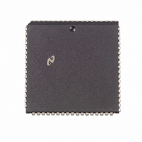
NS32FX164AV-25 National Semiconductor, NS32FX164AV-25 Datasheet - Page 71

NS32FX164AV-25
Manufacturer Part Number
NS32FX164AV-25
Description
IC IMAGING COMM SGNL PROC PLCC68
Manufacturer
National Semiconductor
Datasheet
1.NS32FX164AV-25.pdf
(102 pages)
Specifications of NS32FX164AV-25
Processor Type
Advanced Imaging/Communications Signal Processor SIAP™
Speed
50MHz
Voltage
5V
Mounting Type
Surface Mount
Package / Case
68-PLCC
Lead Free Status / RoHS Status
Contains lead / RoHS non-compliant
Features
-
Other names
*NS32FX164AV-25
Q1284286
Q1284286
Available stocks
Company
Part Number
Manufacturer
Quantity
Price
Company:
Part Number:
NS32FX164AV-25
Manufacturer:
NSC
Quantity:
12 388
Company:
Part Number:
NS32FX164AV-25
Manufacturer:
Texas Instruments
Quantity:
10 000
3 0 Functional Description
3 5 5 10 Instruction Status
In addition to the four bits of Bus Cycle status (ST0– 3) the
NS32FX164 CPU also presents Instruction Status informa-
tion on three separate pins
ST0 –3 in that they are synchronous to the CPU’s internal
instruction execution section rather than to its bus interface
section
PFS (Program Flow Status) is pulsed low as each instruction
begins execution It is intended for debugging purposes
U S originates from the U-bit of the Processor Status Regis-
ter and indicates whether the CPU is currently running in
User or Supervisor mode Although it is not synchronous to
bus cycles there are guarantees on its validity during any
given bus cycle See the Timing Specifications in Section
4 4 2
ILO (Interlocked Operation) is activated during an SBITI (Set
Bit Interlocked) or CBITI (Clear Bit Interlocked) instruction
It is made available to external bus arbitration circuitry in
order to allow these instructions to implement the sema-
phore primitive operations for multi-processor communica-
tion and resource sharing ILO is guaranteed to be active
during the operand accesses performed by the interlocked
instructions
Note The acknowledge of HOLD is on a cycle by cycle basis Therefore it
4 0 Device Specifications
4 1 NS32FX164 PIN DESCRIPTIONS
The following is a brief description of all NS32FX164 pins
The descriptions reference portions of the Functional De-
scription Section 3 0
Note An asterisk next to the signal name indicates a TRI-STATE condition
4 1 1 Supplies
V
GND
4 1 2 Input Signals
RSTI
HOLD
CC
is possible to have HLDA active when an interlock operation is in
progress In this case ILO remains low and the interlocked instruction
continues only after HOLD is de-asserted
for that signal during HOLD acknowledge
Reset Input
Schmitt triggered asynchronous signal used to
generate a CPU reset See Section 3 5 4
Note The reset signal is a true asynchronous input Therefore
Hold Request
When active causes the CPU to release the bus
for DMA or multiprocessing purposes See Sec-
tion 3 5 5 9
Note If the HOLD signal is generated asynchronously its set
Power
Ground
Ground reference for both on-chip logic and
output drivers
a
5V positive supply
no external synchronizing circuit is needed
up and hold times may be violated In this case it is
recommended to synchronize it with CTTL to minimize
the possibility of metastable states
The CPU provides only one synchronization stage to
minimize the HLDA latency This is to avoid speed deg-
radations in cases of heavy HOLD activity (i e DMA
controller cycles interleaved with CPU cycles)
These pins differ from
(Continued)
71
INT
NMI
CWAIT
OSCIN
4 1 3 Output Signals
A16 – A23 High-Order Address Bits
HBE
ST0– 3
U S
ILO
HLDA
PFS
Note INT and NMI are true asynchronous inputs Therefore
Interrupt
A low level on this pin requests a maskable inter-
rupt INT must be kept asserted until the interrupt
is acknowledged
Non-Maskable Interrupt
A High-to-Low transition on this signal requests a
non-maskable interrupt
Continuous Wait
Causes the CPU to insert continuous wait states
if sampled low at the end of T2 and each follow-
ing T-State See Section 3 5 5 3
Crystal External Clock Input
Input from a crystal or an external clock source
See Section 3 5 2
These are the most significant 8 bits of the mem-
ory address bus
Status signal used to enable data transfers on
the most significant byte of the data bus
Status
Bus cycle status code ST0 is the least signifi-
cant Encodings are
0000
0001
0010
0011
0100
0101
0110
0111
1000
1001
1010
1011
1100
1101
1110
1111
User Supervisor
User or Supervisor Mode status High indicates
User Mode low indicates Supervisor Mode
Interlocked Operation
When active indicates that an interlocked opera-
tion is being executed
Hold Acknowledge
Activated by the CPU in response to the HOLD
input to indicate that the CPU has released the
bus
Program Flow Status
A pulse on this signal indicates the beginning of
execution of an instruction
High Byte Enable
no external synchronizing circuit is needed
Idle CPU Inactive on Bus
Idle WAIT Instruction
DSP Module Data Transfer
Idle Waiting for Slave
Interrupt Acknowledge Master
Interrupt Acknowledge Cascaded
End of Interrupt Master
End of Interrupt Cascaded
Sequential Instruction Fetch
Non-Sequential Instruction Fetch
Data Transfer
Read Read-Modify-Write Operand
Read for Effective Address
Transfer Slave Operand
Read Slave Status Word
Broadcast Slave ID


