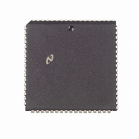
NS32FX164AV-25 National Semiconductor, NS32FX164AV-25 Datasheet - Page 72

NS32FX164AV-25
Manufacturer Part Number
NS32FX164AV-25
Description
IC IMAGING COMM SGNL PROC PLCC68
Manufacturer
National Semiconductor
Datasheet
1.NS32FX164AV-25.pdf
(102 pages)
Specifications of NS32FX164AV-25
Processor Type
Advanced Imaging/Communications Signal Processor SIAP™
Speed
50MHz
Voltage
5V
Mounting Type
Surface Mount
Package / Case
68-PLCC
Lead Free Status / RoHS Status
Contains lead / RoHS non-compliant
Features
-
Other names
*NS32FX164AV-25
Q1284286
Q1284286
Available stocks
Company
Part Number
Manufacturer
Quantity
Price
Company:
Part Number:
NS32FX164AV-25
Manufacturer:
NSC
Quantity:
12 388
Company:
Part Number:
NS32FX164AV-25
Manufacturer:
Texas Instruments
Quantity:
10 000
4 0 Device Specifications
BPU
RSTO
RD
WR
TSO
DBE
OSCOUT Crystal Output
BPU Cycle
This signal is activated during a bus cycle to en-
able an external BITBLT processing unit The
EXTBLT instruction activates this signal
Reset Output
This signal becomes active when RSTI is low
initiating a system reset
Read Strobe
Activated during CPU or DMA read cycles to en-
able reading of data from memory or peripherals
See Section 3 5 5 2
Write Strobe
Activated during CPU or DMA write cycles to en-
able writing of data to memory or peripherals
Timing State Output
The falling edge of TSO identifies the beginning
of state T2 of a bus cycle The rising edge identi-
fies the beginning of state T4
Data Buffers Enable
Used to control external data buffers It is active
when the data buffers are to be enabled
This line is used as the return path for the crystal
(if used) When an external clock source is used
OSCOUT should be left unconnected or loaded
with no more than 5 pF of stray capacitance
Note BPU is low (Active) only during bus cycles involving pre-
fetching instructions and execution of EXTBLT oper-
ands It is recommended that BPU ADS and status lines
(ST0–ST3) be used to qualify BPU bus cycles If a DMA
circuit exists in the system the HLDA signal should be
used to further qualify BPU cycles BPU may become
active during T4 of a non-BPU bus cycle and may be-
come inactive during T4 of a BPU bus cycle BPU must
be qualified by ADS and status lines (ST0–ST3) to be
used as an external gating signal
(Continued)
72
IAS
CTTL1– 2 System Clock
FCLK
ALE
IOUT
4 1 4 Input-Output Signals
AD0 –15
SPC
DDIN
ADS
Special Cycle Address Strobe
Signals the beginning of a special bus cycle
Output clock for bus timing CTTL1 and CTTL2
must be externally connected together
Fast Clock
This clock is derived from the clock waveform on
OSCIN Its frequency is either the same as
OSCIN or is lower depending upon the scale fac-
tor programmed into the CFG register
Address Latch Enable
Active high signal that can be used to control
external address latches
Interrupt Output
Activated when the execution of a command list
stops and the associated interrupt is enabled
Multiplexed Address Data Information Bit 0 is
the least significant bit of each
Slave Processor Control
Used by the CPU as the data strobe output for
slave processor transfers used by a slave proc-
essor to acknowledge completion of a slave in-
struction See Section 3 5 5 7
Status signal indicating the directon of the data
transfer during a bus cycle During HOLD ac-
knowledge this signal becomes an input and de-
termines the activation of RD or WR
Controls address latches signals the beginning
of a bus cycle During HOLD acknowledge this
signal becomes an input and the CPU monitors it
to detect the beginning of a DMA cycle and gen-
erate the relevant strobe signals When a DMA is
used ADS should be pulled up to V
10 k
Address Data Bus
Data Direction
Address Strobe
resistor
CC
through a


