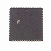
NS32FX164AV-25 National Semiconductor, NS32FX164AV-25 Datasheet - Page 62

NS32FX164AV-25
Manufacturer Part Number
NS32FX164AV-25
Description
IC IMAGING COMM SGNL PROC PLCC68
Manufacturer
National Semiconductor
Datasheet
1.NS32FX164AV-25.pdf
(102 pages)
Specifications of NS32FX164AV-25
Processor Type
Advanced Imaging/Communications Signal Processor SIAP™
Speed
50MHz
Voltage
5V
Mounting Type
Surface Mount
Package / Case
68-PLCC
Lead Free Status / RoHS Status
Contains lead / RoHS non-compliant
Features
-
Other names
*NS32FX164AV-25
Q1284286
Q1284286
Available stocks
Company
Part Number
Manufacturer
Quantity
Price
Company:
Part Number:
NS32FX164AV-25
Manufacturer:
NSC
Quantity:
12 388
Company:
Part Number:
NS32FX164AV-25
Manufacturer:
Texas Instruments
Quantity:
10 000
3 0 Functional Description
At this time the signals TSO (Timing State Output) DBE
(Data Buffer Enable) and either RD (Read Strobe) or WR
(Write Strobe) will also be activated
The T3 state provides for access time requirements and it
occurs at least once in a bus cycle At the end of T2 on the
rising edge of CTTL the CWAIT signal is sampled to deter-
mine whether the bus cycle will be extended See Section
3 5 5 3
If the CPU is performing a read cycle the data bus (AD0–
AD15) is sampled at the beginning of T4 on the rising edge
of CTTL Data must however be held a little longer to meet
the data hold time requirements The RD signal is guaran-
teed not to go inactive before this time so its rising edge
can be safely used to disable the device providing the input
data
The T4 state finishes the bus cycle At the beginning of T4
the RD or WR and TSO signals go inactive and on the
falling edge of CTTL DBE goes inactive having provided for
necessary data hold times Data during Write cycles re-
mains valid from the CPU throughout T4 Note that the Bus
Status lines (ST0–ST3) change at the beginning of T4 an-
ticipating the following bus cycle (if any)
3 5 5 3 Cycle Extension
To allow sufficient access time for any speed of memory or
peripheral device the NS32FX164 provides for extension of
(Continued)
62
Figure 3-23 shows a bus cycle extended by three wait
a bus cycle Any type of bus cycle except a Slave Processor
cycle and a special bus cycle can be extended
In Figures 3-21 and 3-22 note that during T3 all bus control
signals from the CPU are flat Therefore a bus cycle can be
cleanly extended by causing the T3 state to be repeated
This is the purpose of the CWAIT input signal
At the end of state T2 on the rising edge of CTTL CWAIT is
sampled
CWAIT causes wait states to be inserted continuously as
long as it is sampled active It is normally used when the
number of wait states to be inserted in the CPU bus cycle is
not known in advance
The following sequence shows the CPU response to the
WAIT1– 2 and CWAIT inputs
1 Start bus cycle
2 Sample CWAIT at the end of state T2
3 If CWAIT is not active then go to step 6
4 Insert one wait state
5 Sample CWAIT again then go to step 3
6 Complete bus cycle
states due to CWAIT


