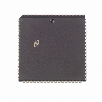
NS32FX164AV-25 National Semiconductor, NS32FX164AV-25 Datasheet - Page 65

NS32FX164AV-25
Manufacturer Part Number
NS32FX164AV-25
Description
IC IMAGING COMM SGNL PROC PLCC68
Manufacturer
National Semiconductor
Datasheet
1.NS32FX164AV-25.pdf
(102 pages)
Specifications of NS32FX164AV-25
Processor Type
Advanced Imaging/Communications Signal Processor SIAP™
Speed
50MHz
Voltage
5V
Mounting Type
Surface Mount
Package / Case
68-PLCC
Lead Free Status / RoHS Status
Contains lead / RoHS non-compliant
Features
-
Other names
*NS32FX164AV-25
Q1284286
Q1284286
Available stocks
Company
Part Number
Manufacturer
Quantity
Price
Company:
Part Number:
NS32FX164AV-25
Manufacturer:
NSC
Quantity:
12 388
Company:
Part Number:
NS32FX164AV-25
Manufacturer:
Texas Instruments
Quantity:
10 000
3 0 Functional Description
3 5 5 6 Special Bus Cycles
Special bus cycles are performed during CPU accesses to
the DSP Module (DSPM) registers or internal RAM These
cycles may be used by external logic to track CPU activities
involving on-chip bus transactions
A special bus cycle starts with the assertion of the special
output signal IAS The ALE signal stays high during the en-
tire cycle and the signals ADS TSO DBE RD and WR are
not activated CWAIT is ignored
A CPU access to a DSP Module register or internal RAM
occurring while a vector operation is being executed is de-
layed until the end of the vector operation This delay can-
not be observed externally
The CPU drives the data bus with the same data that is
being written into the on-chip register or RAM during a spe-
FIGURE 3-24 Special Bus Cycle Timing
(Continued)
65
cial write cycle and ignores the data placed on the data bus
during a special read cycle The 24 least significant address
bits of the DSPM register being accessed are output on the
AD0 – AD15 and A16– A23 signals Figure 3-24 shows the
timing for special read and write cycles
3 5 5 7 Slave Processor Bus Cycles
A Slave Processor bus cycle always takes exactly two clock
cycles labeled T1 and T4 (see Figures 3-25 and 3-26 )
During a Read cycle SPC is active from the beginning of T1
to the beginning of T4 and the data is sampled at the end of
T1 The Cycle Status pins lead the cycle by one clock peri-
od and are sampled on the leading edge of SPC During a
Write cycle the CPU applies data and activates SPC at T1
removing SPC at T4 The Slave Processor latches the
status on the leading edge of SPC and latches data on the
trailing edge
TL EE 11267 – 36


