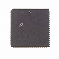
NS32FX164AV-25 National Semiconductor, NS32FX164AV-25 Datasheet - Page 92

NS32FX164AV-25
Manufacturer Part Number
NS32FX164AV-25
Description
IC IMAGING COMM SGNL PROC PLCC68
Manufacturer
National Semiconductor
Datasheet
1.NS32FX164AV-25.pdf
(102 pages)
Specifications of NS32FX164AV-25
Processor Type
Advanced Imaging/Communications Signal Processor SIAP™
Speed
50MHz
Voltage
5V
Mounting Type
Surface Mount
Package / Case
68-PLCC
Lead Free Status / RoHS Status
Contains lead / RoHS non-compliant
Features
-
Other names
*NS32FX164AV-25
Q1284286
Q1284286
Available stocks
Company
Part Number
Manufacturer
Quantity
Price
Company:
Part Number:
NS32FX164AV-25
Manufacturer:
NSC
Quantity:
12 388
Company:
Part Number:
NS32FX164AV-25
Manufacturer:
Texas Instruments
Quantity:
10 000
Appendix B Instruction Execution Times
This section provides the necessary information to calculate
the instruction execution times for the NS32FX164
The following assumptions are made
Y
Y
Y
Y
Y
B 1 BASIC AND FLOATING-POINT INSTRUCTIONS
Execution times for basic and floating-point instructions are
given in Tables B-1 and B-2 The parameters needed for the
various calculations are defined below
TOPW
NCYC
TOPD
TOPB
TFPU
TEA1
TEA2
TOPi
TEA
TCY
TPR
The entire instruction with all displacements and imme-
diate operands is assumed to be present in the instruc-
tion queue when needed
Interference from instruction prefetches which is very
dependent upon the preceding instruction(s) is ignored
This assumption will tend to affect the timing estimate
in an optimistic direction
It is assumed that all memory operand transfers are
completed before the next instruction begins execution
In the case of an operand of access class rmw in
memory this is pessimistic as the Write transfer occurs
in parallel with the execution of the next instruction
It is assumed that there is no overlap between the
fetch of an operand and the following sequences of mi-
crocode This is pessimistic as the fetch of Operand 1
will generally occur in parallel with the effective address
calculation of Operand 2 and the fetch of Operand 2
will occur in parallel with the execution phase of the in-
struction
Where possible the values of operands are taken into
consideration when they affect instruction timing and a
range of times is given Where this is not done the
worst case is assumed
L
The time required to calculate an operand’s Effec-
tive Address For a Register or Immediate oper-
and this includes the fetch of that operand
TEA value for the GEN or GEN1 operand
TEA value for the GEN2 operand
The time needed to read or write a memory byte
The time needed to read or write a memory word
The time needed to read or write a memory dou-
ble-word
The time needed to read or write a memory oper-
and where the operand size is given by the opera-
tion length of the instruction It is always equiva-
lent to either TOPB TOPW or TOPD
Internal processing overhead in clock cycles
Internal processing whose duration depends on
the operation length The number of clock cycles
is derived by multiplying this value by the number
of bytes in the operation length
Number of bus cycles performed by the CPU to
fetch or store an operand NCYC depends on the
operand size and alignment
CPU processing (in clock cycles) performed in par-
allel with the FPU
Processing time required by the FPU to execute
the instruction This is the time from the last data
sent to the FPU until done is issued TFPU can be
found in the FPU data sheets
92
B 1 1 Equations
The following equations assume that
Note When multiple writes are performed during the execution of an in-
TEA
TI1
TI2 depends on the scale factor
TOPW
TOPB
TOPD
IMMEDIATE
ABSOLUTE
EXTERNAL
MEMORY RELATIVE
REGISTER
REGISTER RELATIVE
MEMORY SPACE
TOP OF STACK
SCALED INDEXED
Memory accesses occur at full speed
Any wait states should be reflected in the calculations of
TOPB TOPW and TOPD
e
Tf
Ti
struction wait states occurring during intermediate write transactions
may be partially hidden by the internal execution Therefore a certain
number of wait states can be inserted with no effect on the execution
time For example in the case of the MOVSi instructions each wait
state on write operations subtracts 1 clock cycle per write bus access
from the TCY of the instruction since updating the pointers occurs in
parallel with the write operation This means that wait states can be
added to write cycles without changing the execution time of the in-
struction up to a maximum of 13 wait states on writes for MOVSB and
MOVSW and 4 wait states on writes for MOVSD
Addressing
f
TEA of the basemode except
TEA values for the various addressing modes are
provided in the following table
Mode
This parameter is related to the floating-point op-
erand size
The time required to transfer 32 bits of floating
point value to or from the FPU
The time required to transfer an integer value to or
from the FPU
if basemode is REGISTER then TI1
if basemode is TOP OF STACK then TI1
if byte indexing TI1
if word indexing TI2
if double-word indexing TI2
if quad-word indexing TI2
If operand is in a register or is immediate then
TOPB
else TOPB
If operand is in a register or is immediate then
TOPW
else TOPW
If operand is in a register or is immediate then
TOPD
else TOPD
e
e
e
0
0
0
e
e
e
TEA TABLE
11
3
4
4
7
TI1
a
a
NCYC
Value
NCYC
TEA
e
2 TOPD
e
a
4
TOPD
2
5
4
2
3
5
TI2
7
b
b
e
e
1
1
10
Access Class Write
Access Class Read
Access Class RMW
8
e
Notes
5
e
4


