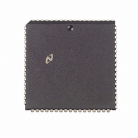
NS32FX164AV-25 National Semiconductor, NS32FX164AV-25 Datasheet - Page 9

NS32FX164AV-25
Manufacturer Part Number
NS32FX164AV-25
Description
IC IMAGING COMM SGNL PROC PLCC68
Manufacturer
National Semiconductor
Datasheet
1.NS32FX164AV-25.pdf
(102 pages)
Specifications of NS32FX164AV-25
Processor Type
Advanced Imaging/Communications Signal Processor SIAP™
Speed
50MHz
Voltage
5V
Mounting Type
Surface Mount
Package / Case
68-PLCC
Lead Free Status / RoHS Status
Contains lead / RoHS non-compliant
Features
-
Other names
*NS32FX164AV-25
Q1284286
Q1284286
Available stocks
Company
Part Number
Manufacturer
Quantity
Price
Company:
Part Number:
NS32FX164AV-25
Manufacturer:
NSC
Quantity:
12 388
Company:
Part Number:
NS32FX164AV-25
Manufacturer:
Texas Instruments
Quantity:
10 000
2 0 Architectural Description
B Reserved for use by the CPU This bit is set to 1 during
Note 1 When an interrupt is acknowledged the B I P S and U bits are set
Note 2 If BITBLT (BB) or EXTBLT instructions are executed in an interrupt
2 1 4 Configuration Register
The Configuration Register (CFG) is 32 bits wide of which 5
bits are implemented The implemented bits enable various
operating modes for the CPU including vectoring of inter-
rupts execution of floating-point instructions processing of
exceptions and selection of clock scaling factor The CFG is
programmed by the SETCFG instruction The format of CFG
is shown in Figure 2-3 The various control bits are de-
scribed below
I
F
M
C
DE Direct-Exception mode enable This bit enables the Di-
2 1 5 DSP Module Registers
The DSP Module (DSPM) contains 15 memory-mapped reg-
isters All the registers except OVF CLSTAT ABORT
DSPINT and NMISTAT are readable and writable OVF
CLSTAT DSPINT and NMISTAT are read-only ABORT is
write-only
The DSPM registers are divided into two groups according
to their function PARAM OVF X Y Z A REPEAT CLPTR
and EABR are called DSPM dedicated registers CLSTAT
ABORT DSPINT DSPMASK EXT and NMISTAT are called
CPU core interface registers
Accesses to these registers must be aligned word and dou-
ble-word accesses must occur on word and double-word
address boundaries respectively Failing to do so will cause
unpredictable results Figure 2-4 shows the address map of
the DSP Module registers
31
the execution of the EXTBLT instruction and causes the
BPU signal to become active Upon reset B is set to
zero and the BPU signal is set high
Interrupt vectoring This bit controls whether maskable
interrupts are handled in nonvectored (I
tored (I
formation
Floating-point instruction set This bit indicates wheth-
er a floating-point unit (FPU) is present to execute
floating-point instructions If this bit is 0 when the CPU
executes a floating-point instruction a Trap (UND) oc-
curs If this bit is 1 then the CPU transfers the instruc-
tion and any necessary operands to the FPU using the
slave-processor protocol described in Section 3 1 3 1
Clock scaling This bit is used in conjunction with the
C-bit to select the clock scaling factor
Clock scaling Same as the M-bit above Refer to Sec-
tion 3 5 3 on ‘‘Power Save Mode’’ for details
rect-Exception mode for processing exceptions When
this mode is selected the CPU response time to inter-
rupts and other exceptions is significantly improved
Refer to Section 3 2 for more information
to zero and the BPU signal is set high A return from interrupt will
restore the original values from the copy of the PSR register saved
in the interrupt stack
routine the PSR bits J and K must be cleared first
FIGURE 2-3 Configuration Register (CFG)
Reserved
e
1) mode Refer to Section 3 2 3 for more in-
DE
8
7
Res
C M F
e
(Continued)
0) or vec-
0
I
9
A Accumulator
The format of the accumulator is shown in Figure 2-5
The A register is a complex accumulator It has two 34-bit
fields a real part and an imaginary part Bits 15 through 30
of the real and the imaginary parts of the accumulator can
be read or written by the core in one double-word access
Bits 15 through 30 of the real part are mapped to the oper-
and’s bits 0 through 15 and bits 15 through 30 of the imagi-
nary part are mapped to the operand’s bits 16 through 31
The accumulator can also be read and written by the com-
mand-list execution unit using the SA SEA LA and LEA
instructions (See Section 3 4 for more information)
Note that when a value is stored in the accumulator by the
core the value of PARAM RND bit is copied into bit position
14 of both real and imaginary parts of the accumulator This
technique allows rounding of the accumulator’s value in the
following DSPM instructions (See Section 3 4 5 3 for more
information on rounding)
When the Accumulator is loaded either by the core or by the
LA or LEA instructions bits 31– 33 of the real and the imagi-
nary accumulators are loaded with the values of bit 30 of the
real and the imaginary parts respectively
When the Accumulator is loaded either by the core or by the
LA instruction bits 0– 13 of the real and the imaginary accu-
mulators are loaded with zeros
X Y Z Vector Pointers
The format of X Y and Z registers is shown in Figure 2-6
31
33
ADDRESS
FIGURE 2-4 DSP Module Registers Address Map
DSPMASK
NMISTAT
16 15
Imaginary
FIGURE 2-6 X Y Z Registers Format
Register
REPEAT
CLSTAT
DSPINT
PARAM
ABORT
CLPTR
Name
EABR
FIGURE 2-5 Accumulator Format
OVF
EXT
Y
A
X
Z
Reserved
8 7
WRAP-AROUND
0
33
FFFF800C
FFFF900C
FFFF8000
FFFF8004
FFFF8008
FFFF8010
FFFF8014
FFFF8018
FFFF8020
FFFF8024
FFFF9000
FFFF9004
FFFF9008
FFFF9010
FFFF9014
Register
Address
4 3
Real
INCREMENT
0
0


