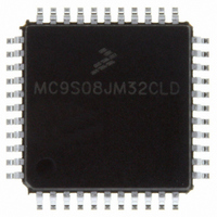
MC9S08JM32CLD Freescale Semiconductor, MC9S08JM32CLD Datasheet - Page 146

MC9S08JM32CLD
Manufacturer Part Number
MC9S08JM32CLD
Description
IC MCU 8BIT 32K FLASH 44-LQFP
Manufacturer
Freescale Semiconductor
Series
HCS08r
Datasheet
1.MC9S08JM32CLD.pdf
(388 pages)
Specifications of MC9S08JM32CLD
Core Processor
HCS08
Core Size
8-Bit
Speed
48MHz
Connectivity
I²C, LIN, SCI, SPI, USB
Peripherals
LVD, POR, PWM, WDT
Number Of I /o
33
Program Memory Size
32KB (32K x 8)
Program Memory Type
FLASH
Ram Size
2K x 8
Voltage - Supply (vcc/vdd)
2.7 V ~ 5.5 V
Data Converters
A/D 8x12b
Oscillator Type
External
Operating Temperature
-40°C ~ 85°C
Package / Case
44-LQFP
Processor Series
S08JM
Core
HCS08
Data Bus Width
8 bit
Data Ram Size
2 KB
Interface Type
SCI/SPI
Maximum Clock Frequency
24 MHz
Number Of Programmable I/os
33
Number Of Timers
8
Maximum Operating Temperature
+ 85 C
Mounting Style
SMD/SMT
3rd Party Development Tools
EWS08
Development Tools By Supplier
DEMOJM, DEMOJMSKT, DEMOFLEXISJMSD, DEMO9S08JM16
Minimum Operating Temperature
- 40 C
On-chip Adc
8-ch x 12-bit
Lead Free Status / RoHS Status
Lead free / RoHS Compliant
Eeprom Size
-
Lead Free Status / Rohs Status
Lead free / RoHS Compliant
Available stocks
Company
Part Number
Manufacturer
Quantity
Price
Company:
Part Number:
MC9S08JM32CLD
Manufacturer:
Freescale Semiconductor
Quantity:
1 948
Company:
Part Number:
MC9S08JM32CLD
Manufacturer:
Freescale Semiconductor
Quantity:
10 000
- Current page: 146 of 388
- Download datasheet (5Mb)
Analog-to-Digital Converter (S08ADC12V1)
10.3.8
The pin control registers disable the I/O port control of MCU pins used as analog inputs. APCTL1 is used
to control the pins associated with channels 0–7 of the ADC module.
146
ADICLK
MODE
Field
3:2
1:0
Reset:
W
R
Pin Control 1 Register (APCTL1)
Conversion Mode Selection. MODE bits are used to select between 12-, 10-, or 8-bit operation. See
Input Clock Select. ADICLK bits select the input clock source to generate the internal clock ADCK. See
Table
ADPC7
10-9.
7
0
Table 10-6. ADCCFG Register Field Descriptions (continued)
ADICLK
MODE
ADIV
00
01
10
11
00
01
10
11
00
01
10
11
ADPC6
0
6
Figure 10-10. Pin Control 1 Register (APCTL1)
8-bit conversion (N=8)
12-bit conversion (N=12)
10-bit conversion (N=10)
Reserved
Bus clock
Bus clock divided by 2
Alternate clock (ALTCLK)
Asynchronous clock (ADACK)
MC9S08JM60 Series Data Sheet, Rev. 3
ADPC5
Table 10-7. Clock Divide Select
Table 10-8. Conversion Modes
Table 10-9. Input Clock Select
0
5
Divide Ratio
1
2
4
8
ADPC4
Selected Clock Source
0
4
Mode Description
Description
ADPC3
0
3
Input clock ÷ 2
Input clock ÷ 4
Input clock ÷ 8
Clock Rate
Input clock
ADPC2
0
2
ADPC1
Freescale Semiconductor
0
1
ADPC0
Table
0
0
10-8.
Related parts for MC9S08JM32CLD
Image
Part Number
Description
Manufacturer
Datasheet
Request
R
Part Number:
Description:
Manufacturer:
Freescale Semiconductor, Inc
Datasheet:
Part Number:
Description:
Manufacturer:
Freescale Semiconductor, Inc
Datasheet:
Part Number:
Description:
Manufacturer:
Freescale Semiconductor, Inc
Datasheet:
Part Number:
Description:
Manufacturer:
Freescale Semiconductor, Inc
Datasheet:
Part Number:
Description:
Manufacturer:
Freescale Semiconductor, Inc
Datasheet:
Part Number:
Description:
Manufacturer:
Freescale Semiconductor, Inc
Datasheet:
Part Number:
Description:
Manufacturer:
Freescale Semiconductor, Inc
Datasheet:
Part Number:
Description:
Manufacturer:
Freescale Semiconductor, Inc
Datasheet:
Part Number:
Description:
Manufacturer:
Freescale Semiconductor, Inc
Datasheet:
Part Number:
Description:
Manufacturer:
Freescale Semiconductor, Inc
Datasheet:
Part Number:
Description:
Manufacturer:
Freescale Semiconductor, Inc
Datasheet:
Part Number:
Description:
Manufacturer:
Freescale Semiconductor, Inc
Datasheet:
Part Number:
Description:
Manufacturer:
Freescale Semiconductor, Inc
Datasheet:
Part Number:
Description:
Manufacturer:
Freescale Semiconductor, Inc
Datasheet:
Part Number:
Description:
Manufacturer:
Freescale Semiconductor, Inc
Datasheet:


