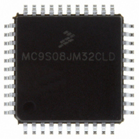
MC9S08JM32CLD Freescale Semiconductor, MC9S08JM32CLD Datasheet - Page 327

MC9S08JM32CLD
Manufacturer Part Number
MC9S08JM32CLD
Description
IC MCU 8BIT 32K FLASH 44-LQFP
Manufacturer
Freescale Semiconductor
Series
HCS08r
Datasheet
1.MC9S08JM32CLD.pdf
(388 pages)
Specifications of MC9S08JM32CLD
Core Processor
HCS08
Core Size
8-Bit
Speed
48MHz
Connectivity
I²C, LIN, SCI, SPI, USB
Peripherals
LVD, POR, PWM, WDT
Number Of I /o
33
Program Memory Size
32KB (32K x 8)
Program Memory Type
FLASH
Ram Size
2K x 8
Voltage - Supply (vcc/vdd)
2.7 V ~ 5.5 V
Data Converters
A/D 8x12b
Oscillator Type
External
Operating Temperature
-40°C ~ 85°C
Package / Case
44-LQFP
Processor Series
S08JM
Core
HCS08
Data Bus Width
8 bit
Data Ram Size
2 KB
Interface Type
SCI/SPI
Maximum Clock Frequency
24 MHz
Number Of Programmable I/os
33
Number Of Timers
8
Maximum Operating Temperature
+ 85 C
Mounting Style
SMD/SMT
3rd Party Development Tools
EWS08
Development Tools By Supplier
DEMOJM, DEMOJMSKT, DEMOFLEXISJMSD, DEMO9S08JM16
Minimum Operating Temperature
- 40 C
On-chip Adc
8-ch x 12-bit
Lead Free Status / RoHS Status
Lead free / RoHS Compliant
Eeprom Size
-
Lead Free Status / Rohs Status
Lead free / RoHS Compliant
Available stocks
Company
Part Number
Manufacturer
Quantity
Price
Company:
Part Number:
MC9S08JM32CLD
Manufacturer:
Freescale Semiconductor
Quantity:
1 948
Company:
Part Number:
MC9S08JM32CLD
Manufacturer:
Freescale Semiconductor
Quantity:
10 000
- Current page: 327 of 388
- Download datasheet (5Mb)
Chapter 18
Development Support
18.1
Introduction
Development support systems in the HCS08 include the background debug controller (BDC) and the
on-chip debug module (DBG). The BDC provides a single-wire debug interface to the target MCU that
provides a convenient interface for programming the on-chip flash and other nonvolatile memories. The
BDC is also the primary debug interface for development and allows non-intrusive access to memory data
and traditional debug features such as CPU register modify, breakpoints, and single instruction trace
commands.
In the HCS08 family, address and data bus signals are not available on external pins (not even in test
modes). Debug is done through commands fed into the target MCU via the single-wire background debug
interface. The debug module provides a means to selectively trigger and capture bus information so an
external development system can reconstruct what happened inside the MCU on a cycle-by-cycle basis
without having external access to the address and data signals.
The alternate BDC clock source for MC9S08JM60 Series is the MCGLCLK. See
Chapter 12,
“Multi-Purpose Clock Generator
(S08MCGV1),” for more information about MCGLCLK and how to
select clock sources.
MC9S08JM60 Series Data Sheet, Rev. 3
Freescale Semiconductor
327
Related parts for MC9S08JM32CLD
Image
Part Number
Description
Manufacturer
Datasheet
Request
R
Part Number:
Description:
Manufacturer:
Freescale Semiconductor, Inc
Datasheet:
Part Number:
Description:
Manufacturer:
Freescale Semiconductor, Inc
Datasheet:
Part Number:
Description:
Manufacturer:
Freescale Semiconductor, Inc
Datasheet:
Part Number:
Description:
Manufacturer:
Freescale Semiconductor, Inc
Datasheet:
Part Number:
Description:
Manufacturer:
Freescale Semiconductor, Inc
Datasheet:
Part Number:
Description:
Manufacturer:
Freescale Semiconductor, Inc
Datasheet:
Part Number:
Description:
Manufacturer:
Freescale Semiconductor, Inc
Datasheet:
Part Number:
Description:
Manufacturer:
Freescale Semiconductor, Inc
Datasheet:
Part Number:
Description:
Manufacturer:
Freescale Semiconductor, Inc
Datasheet:
Part Number:
Description:
Manufacturer:
Freescale Semiconductor, Inc
Datasheet:
Part Number:
Description:
Manufacturer:
Freescale Semiconductor, Inc
Datasheet:
Part Number:
Description:
Manufacturer:
Freescale Semiconductor, Inc
Datasheet:
Part Number:
Description:
Manufacturer:
Freescale Semiconductor, Inc
Datasheet:
Part Number:
Description:
Manufacturer:
Freescale Semiconductor, Inc
Datasheet:
Part Number:
Description:
Manufacturer:
Freescale Semiconductor, Inc
Datasheet:


