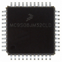
MC9S08JM32CLD Freescale Semiconductor, MC9S08JM32CLD Datasheet - Page 29

MC9S08JM32CLD
Manufacturer Part Number
MC9S08JM32CLD
Description
IC MCU 8BIT 32K FLASH 44-LQFP
Manufacturer
Freescale Semiconductor
Series
HCS08r
Datasheet
1.MC9S08JM32CLD.pdf
(388 pages)
Specifications of MC9S08JM32CLD
Core Processor
HCS08
Core Size
8-Bit
Speed
48MHz
Connectivity
I²C, LIN, SCI, SPI, USB
Peripherals
LVD, POR, PWM, WDT
Number Of I /o
33
Program Memory Size
32KB (32K x 8)
Program Memory Type
FLASH
Ram Size
2K x 8
Voltage - Supply (vcc/vdd)
2.7 V ~ 5.5 V
Data Converters
A/D 8x12b
Oscillator Type
External
Operating Temperature
-40°C ~ 85°C
Package / Case
44-LQFP
Processor Series
S08JM
Core
HCS08
Data Bus Width
8 bit
Data Ram Size
2 KB
Interface Type
SCI/SPI
Maximum Clock Frequency
24 MHz
Number Of Programmable I/os
33
Number Of Timers
8
Maximum Operating Temperature
+ 85 C
Mounting Style
SMD/SMT
3rd Party Development Tools
EWS08
Development Tools By Supplier
DEMOJM, DEMOJMSKT, DEMOFLEXISJMSD, DEMO9S08JM16
Minimum Operating Temperature
- 40 C
On-chip Adc
8-ch x 12-bit
Lead Free Status / RoHS Status
Lead free / RoHS Compliant
Eeprom Size
-
Lead Free Status / Rohs Status
Lead free / RoHS Compliant
Available stocks
Company
Part Number
Manufacturer
Quantity
Price
Company:
Part Number:
MC9S08JM32CLD
Manufacturer:
Freescale Semiconductor
Quantity:
1 948
Company:
Part Number:
MC9S08JM32CLD
Manufacturer:
Freescale Semiconductor
Quantity:
10 000
- Current page: 29 of 388
- Download datasheet (5Mb)
Freescale Semiconductor
NOTES:
1. External crystal circuity is not required if using the MCG internal clock option. For USB operation, an external crystal is required.
2. XTAL and EXTAL are the same pins as PTG4 and PTG5, respectively.
3. RC filters on RESET and IRQ are recommended for EMC-sensitive applications.
4. R
5. V
6. USBDP and USBDN are powered by the 3.3-V regulator or external 3.3-V supply on V
V
The voltage regulator output is used for R
DD
PUDP
BUS
SYSTEM
POWER
NOTE 1
BACKGROUND HEADER
OPTIONAL
is a 5.0-V supply from upstream port that can be used for USB operation
MANUAL
RESET
is shown for full-speed USB only. The diagram shows a configuration where the on-chip regulator and R
C1
USB SERIES-B CONNECTOR
5 V
+
ASYNCHRONOUS
10 μF
INTERRUPT
C
X1
INPUT
BLK
3.3-V Reference
4.7 μF
V
+
R
DD
F
2
3
+
1
4
V
C2
DD
4.7 kΩ–10 kΩ
0.1 μF
C
Figure 2-4. Basic System Connections
0.1 μF
BY
V
MC9S08JM60 Series Data Sheet, Rev. 3
Bus
C
0.1 μF
BYAD
R
PUDP.
S
V
0.47 μF
DD
4.7 kΩ–
10 kΩ
0.1 μF
R
PUDP
V
USBDN
V
can optionally be disabled if using an external pullup resistor on USBDP
V
USB33
V
V
V
V
V
XTAL
USB33
EXTAL
V
REFL
REFH
DDAD
DD
SSAD
SS
SSOSC
R
BKGD/MS
PUDP
RESET
IRQ
USBDP
MC9S08JM60
PORT
PORT
PORT
PORT
PORT
PORT
PORT
B
C
D
E
G
A
F
USB33
.
Chapter 2 Pins and Connections
PTA0–PTA5
PTB0/MISO2/ADP0
PTB1/MOSI2/ADP1
PTB2/SPSCK2/ADP2
PTB3/SS2/ADP3
PTB4/KBIP4/ADP4
PTB5/KBIP5/ADP5
PTB6/ADP6
PTB7/ADP7
PTC0/SCL
PTC1/SDA
PTC2
PTC3/TxD2
PTC4
PTC5/RxD2
PTC6
PTD0/ADP8/ACMP+
PTD1/ADP9/ACMP–
PTD2/KBIP2/ACMPO
PTD3/KBIP3/ADP10
PTD4/ADP11
PTD5
PTD6
PTD7
PTE0/TxD1
PTE1/RxD1
PTE2/TPM1CH0
PTE3/TPM1CH1
PTE4/MISO1
PTE5/MOSI1
PTE6/SPSCK1
PTE7/SS1
PTF0/TPM1CH2
PTF1/TPM1CH3
PTF2/TPM1CH4
PTF3/TPM1CH5
PTF4/TPM2CH0
PTF5/TPM2CH1
PTF6
PTF7
PTG0/KBIP0
PTG1/KBIP1
PTG2/KBIP6
PTG3/KBIP7
PTG4/XTAL
PTG5/EXTAL
PUDP
are enabled.
INTERFACE TO
APPLICATION
PERIPHERAL
SYSTEM
I/O AND
29
Related parts for MC9S08JM32CLD
Image
Part Number
Description
Manufacturer
Datasheet
Request
R
Part Number:
Description:
Manufacturer:
Freescale Semiconductor, Inc
Datasheet:
Part Number:
Description:
Manufacturer:
Freescale Semiconductor, Inc
Datasheet:
Part Number:
Description:
Manufacturer:
Freescale Semiconductor, Inc
Datasheet:
Part Number:
Description:
Manufacturer:
Freescale Semiconductor, Inc
Datasheet:
Part Number:
Description:
Manufacturer:
Freescale Semiconductor, Inc
Datasheet:
Part Number:
Description:
Manufacturer:
Freescale Semiconductor, Inc
Datasheet:
Part Number:
Description:
Manufacturer:
Freescale Semiconductor, Inc
Datasheet:
Part Number:
Description:
Manufacturer:
Freescale Semiconductor, Inc
Datasheet:
Part Number:
Description:
Manufacturer:
Freescale Semiconductor, Inc
Datasheet:
Part Number:
Description:
Manufacturer:
Freescale Semiconductor, Inc
Datasheet:
Part Number:
Description:
Manufacturer:
Freescale Semiconductor, Inc
Datasheet:
Part Number:
Description:
Manufacturer:
Freescale Semiconductor, Inc
Datasheet:
Part Number:
Description:
Manufacturer:
Freescale Semiconductor, Inc
Datasheet:
Part Number:
Description:
Manufacturer:
Freescale Semiconductor, Inc
Datasheet:
Part Number:
Description:
Manufacturer:
Freescale Semiconductor, Inc
Datasheet:


