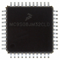
MC9S08JM32CLD Freescale Semiconductor, MC9S08JM32CLD Datasheet - Page 74

MC9S08JM32CLD
Manufacturer Part Number
MC9S08JM32CLD
Description
IC MCU 8BIT 32K FLASH 44-LQFP
Manufacturer
Freescale Semiconductor
Series
HCS08r
Datasheet
1.MC9S08JM32CLD.pdf
(388 pages)
Specifications of MC9S08JM32CLD
Core Processor
HCS08
Core Size
8-Bit
Speed
48MHz
Connectivity
I²C, LIN, SCI, SPI, USB
Peripherals
LVD, POR, PWM, WDT
Number Of I /o
33
Program Memory Size
32KB (32K x 8)
Program Memory Type
FLASH
Ram Size
2K x 8
Voltage - Supply (vcc/vdd)
2.7 V ~ 5.5 V
Data Converters
A/D 8x12b
Oscillator Type
External
Operating Temperature
-40°C ~ 85°C
Package / Case
44-LQFP
Processor Series
S08JM
Core
HCS08
Data Bus Width
8 bit
Data Ram Size
2 KB
Interface Type
SCI/SPI
Maximum Clock Frequency
24 MHz
Number Of Programmable I/os
33
Number Of Timers
8
Maximum Operating Temperature
+ 85 C
Mounting Style
SMD/SMT
3rd Party Development Tools
EWS08
Development Tools By Supplier
DEMOJM, DEMOJMSKT, DEMOFLEXISJMSD, DEMO9S08JM16
Minimum Operating Temperature
- 40 C
On-chip Adc
8-ch x 12-bit
Lead Free Status / RoHS Status
Lead free / RoHS Compliant
Eeprom Size
-
Lead Free Status / Rohs Status
Lead free / RoHS Compliant
Available stocks
Company
Part Number
Manufacturer
Quantity
Price
Company:
Part Number:
MC9S08JM32CLD
Manufacturer:
Freescale Semiconductor
Quantity:
1 948
Company:
Part Number:
MC9S08JM32CLD
Manufacturer:
Freescale Semiconductor
Quantity:
10 000
- Current page: 74 of 388
- Download datasheet (5Mb)
1
Chapter 5 Resets, Interrupts, and System Configuration
5.7.3
This register contains a single write-only control bit. A serial background command such as
WRITE_BYTE must be used to write to SBDFR. Attempts to write this register from a user program are
ignored. Reads always return 0x00.
5.7.4
This register may be read at any time. Bits 3 and 2 are unimplemented and always read 0. This is a
write-once register so only the first write after reset is honored. Any subsequent attempt to write to SOPT
(intentionally or unintentionally) is ignored to avoid accidental changes to these sensitive settings. SOPT
74
BDFR is writable only through serial background debug commands, not from user programs.
Reset
BDFR
Field
Field
ILOP
COP
LOC
LVD
5
4
2
1
0
W
R
System Background Debug Force Reset Register (SBDFR)
System Options Register 1 (SOPT1)
Computer Operating Properly (COP) Watchdog — Reset was caused by the COP watchdog timer timing out.
This reset source may be blocked by COPE = 0.
0 Reset not caused by COP timeout.
1 Reset caused by COP timeout.
Illegal Opcode — Reset was caused by an attempt to execute an unimplemented or illegal opcode. The STOP
instruction is considered illegal if stop is disabled by STOPE = 0 in the SOPT register. The BGND instruction is
considered illegal if active background mode is disabled by ENBDM = 0 in the BDCSC register.
0 Reset not caused by an illegal opcode.
1 Reset caused by an illegal opcode.
Loss-of-Clock Reset — Reset was caused by a loss of external clock.
0 Reset not caused by a loss of external clock.
1 Reset caused by a loss of external clock.
Low Voltage Detect — If the LVD is enable with the LVDRE or LVDSE bit is set, and the supply drops below the
LVD trip voltage, an LVD reset will occur. This bit is also set by POR.
0 Reset not caused by LVD trip or POR.
1 Reset caused by LVD trip or POR.
Background Debug Force Reset — A serial background command such as WRITE_BYTE may be used to
allow an external debug host to force a target system reset. Writing logic 1 to this bit forces an MCU reset. This
bit cannot be written from a user program.
0
0
7
Figure 5-4. System Background Debug Force Reset Register (SBDFR)
= Unimplemented or Reserved
Table 5-3. SRS Register Field Descriptions (continued)
0
0
6
Table 5-4. SBDFR Register Field Descriptions
MC9S08JM60 Series Data Sheet, Rev. 3
0
0
5
0
0
4
Description
Description
3
0
0
0
0
2
Freescale Semiconductor
0
0
1
BDFR
0
0
0
1
Related parts for MC9S08JM32CLD
Image
Part Number
Description
Manufacturer
Datasheet
Request
R
Part Number:
Description:
Manufacturer:
Freescale Semiconductor, Inc
Datasheet:
Part Number:
Description:
Manufacturer:
Freescale Semiconductor, Inc
Datasheet:
Part Number:
Description:
Manufacturer:
Freescale Semiconductor, Inc
Datasheet:
Part Number:
Description:
Manufacturer:
Freescale Semiconductor, Inc
Datasheet:
Part Number:
Description:
Manufacturer:
Freescale Semiconductor, Inc
Datasheet:
Part Number:
Description:
Manufacturer:
Freescale Semiconductor, Inc
Datasheet:
Part Number:
Description:
Manufacturer:
Freescale Semiconductor, Inc
Datasheet:
Part Number:
Description:
Manufacturer:
Freescale Semiconductor, Inc
Datasheet:
Part Number:
Description:
Manufacturer:
Freescale Semiconductor, Inc
Datasheet:
Part Number:
Description:
Manufacturer:
Freescale Semiconductor, Inc
Datasheet:
Part Number:
Description:
Manufacturer:
Freescale Semiconductor, Inc
Datasheet:
Part Number:
Description:
Manufacturer:
Freescale Semiconductor, Inc
Datasheet:
Part Number:
Description:
Manufacturer:
Freescale Semiconductor, Inc
Datasheet:
Part Number:
Description:
Manufacturer:
Freescale Semiconductor, Inc
Datasheet:
Part Number:
Description:
Manufacturer:
Freescale Semiconductor, Inc
Datasheet:


