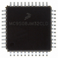
MC9S08JM32CLD Freescale Semiconductor, MC9S08JM32CLD Datasheet - Page 354

MC9S08JM32CLD
Manufacturer Part Number
MC9S08JM32CLD
Description
IC MCU 8BIT 32K FLASH 44-LQFP
Manufacturer
Freescale Semiconductor
Series
HCS08r
Datasheet
1.MC9S08JM32CLD.pdf
(388 pages)
Specifications of MC9S08JM32CLD
Core Processor
HCS08
Core Size
8-Bit
Speed
48MHz
Connectivity
I²C, LIN, SCI, SPI, USB
Peripherals
LVD, POR, PWM, WDT
Number Of I /o
33
Program Memory Size
32KB (32K x 8)
Program Memory Type
FLASH
Ram Size
2K x 8
Voltage - Supply (vcc/vdd)
2.7 V ~ 5.5 V
Data Converters
A/D 8x12b
Oscillator Type
External
Operating Temperature
-40°C ~ 85°C
Package / Case
44-LQFP
Processor Series
S08JM
Core
HCS08
Data Bus Width
8 bit
Data Ram Size
2 KB
Interface Type
SCI/SPI
Maximum Clock Frequency
24 MHz
Number Of Programmable I/os
33
Number Of Timers
8
Maximum Operating Temperature
+ 85 C
Mounting Style
SMD/SMT
3rd Party Development Tools
EWS08
Development Tools By Supplier
DEMOJM, DEMOJMSKT, DEMOFLEXISJMSD, DEMO9S08JM16
Minimum Operating Temperature
- 40 C
On-chip Adc
8-ch x 12-bit
Lead Free Status / RoHS Status
Lead free / RoHS Compliant
Eeprom Size
-
Lead Free Status / Rohs Status
Lead free / RoHS Compliant
Available stocks
Company
Part Number
Manufacturer
Quantity
Price
Company:
Part Number:
MC9S08JM32CLD
Manufacturer:
Freescale Semiconductor
Quantity:
1 948
Company:
Part Number:
MC9S08JM32CLD
Manufacturer:
Freescale Semiconductor
Quantity:
10 000
- Current page: 354 of 388
- Download datasheet (5Mb)
Appendix A Electrical Characteristics
354
1
2
3
4
5
6
7
8
Num C
19
20
21
22
23
24
25
26
Typical values are based on characterization data at 25°C unless otherwise stated.
Maximum is highest voltage that POR is guaranteed.
Measured with V
Measured with V
Power supply must maintain regulation within operating V
maximum current conditions. If positive injection current (V
flow out of V
shunt current greater than maximum injection current. This will be the greatest risk when the MCU is not
consuming power. Examples are: if no system clock is present, or if clock rate is very low (which would reduce
overall power consumption).
All functional non-supply pins are internally clamped to V
Input must be current limited to the value specified. To determine the value of the required current-limiting
resistor, calculate resistance values for positive and negative clamp voltages, then use the larger of the two
values.
The RESET pin does not have a clamp diode to V
P
P
P
C
P
C
P
T
Low-voltage detection threshold —
High range
Low-voltage detection threshold —
Low range
Low-voltage warning threshold —
High range 1
Low-voltage warning threshold —
High range 0
Low-voltage warning threshold
Low range 1
Low-voltage warning threshold —
Low range 0
Low-voltage inhibit reset/recover hysteresis
Bandgap voltage reference
factory trimmed at V
DD
and could result in external power supply going out of regulation. Ensure external V
In
In
= V
= V
SS
DD
.
.
Parameter
DD
Table A-6. DC Characteristics (continued)
= 5.0 V, Temp = 25°C
MC9S08JM60 Series Data Sheet, Rev. 3
V
V
V
V
V
V
V
V
V
V
V
V
DD
DD
DD
DD
DD
DD
DD
DD
DD
DD
DD
DD
DD
falling
falling
falling
falling
falling
falling
rising
rising
rising
rising
rising
rising
. Do not drive this pin above V
+5V
+3V
SS
DD
In
Symbol
> V
V
V
V
V
and V
V
V
range during instantaneous and operating
V
V
LVW3
LVW2
LVW1
LVW0
LVD1
LVD0
hys
BG
DD
) is greater than I
DD
.
2.48
2.54
2.84
2.90
2.66
2.72
1.19
Min
3.9
4.0
4.5
4.6
4.2
4.3
—
—
Typical
DD
DD
2.56
2.62
2.92
2.98
2.74
2.80
1.20
100
4.0
4.1
4.6
4.7
4.3
4.4
60
, the injection current may
.
1
Freescale Semiconductor
Max.
2.64
2.70
3.00
3.06
2.82
2.88
1.21
4.1
4.2
4.7
4.8
4.4
4.5
—
—
DD
load will
Unit
mV
mV
V
V
V
V
V
V
V
Related parts for MC9S08JM32CLD
Image
Part Number
Description
Manufacturer
Datasheet
Request
R
Part Number:
Description:
Manufacturer:
Freescale Semiconductor, Inc
Datasheet:
Part Number:
Description:
Manufacturer:
Freescale Semiconductor, Inc
Datasheet:
Part Number:
Description:
Manufacturer:
Freescale Semiconductor, Inc
Datasheet:
Part Number:
Description:
Manufacturer:
Freescale Semiconductor, Inc
Datasheet:
Part Number:
Description:
Manufacturer:
Freescale Semiconductor, Inc
Datasheet:
Part Number:
Description:
Manufacturer:
Freescale Semiconductor, Inc
Datasheet:
Part Number:
Description:
Manufacturer:
Freescale Semiconductor, Inc
Datasheet:
Part Number:
Description:
Manufacturer:
Freescale Semiconductor, Inc
Datasheet:
Part Number:
Description:
Manufacturer:
Freescale Semiconductor, Inc
Datasheet:
Part Number:
Description:
Manufacturer:
Freescale Semiconductor, Inc
Datasheet:
Part Number:
Description:
Manufacturer:
Freescale Semiconductor, Inc
Datasheet:
Part Number:
Description:
Manufacturer:
Freescale Semiconductor, Inc
Datasheet:
Part Number:
Description:
Manufacturer:
Freescale Semiconductor, Inc
Datasheet:
Part Number:
Description:
Manufacturer:
Freescale Semiconductor, Inc
Datasheet:
Part Number:
Description:
Manufacturer:
Freescale Semiconductor, Inc
Datasheet:


