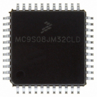
MC9S08JM32CLD Freescale Semiconductor, MC9S08JM32CLD Datasheet - Page 230

MC9S08JM32CLD
Manufacturer Part Number
MC9S08JM32CLD
Description
IC MCU 8BIT 32K FLASH 44-LQFP
Manufacturer
Freescale Semiconductor
Series
HCS08r
Datasheet
1.MC9S08JM32CLD.pdf
(388 pages)
Specifications of MC9S08JM32CLD
Core Processor
HCS08
Core Size
8-Bit
Speed
48MHz
Connectivity
I²C, LIN, SCI, SPI, USB
Peripherals
LVD, POR, PWM, WDT
Number Of I /o
33
Program Memory Size
32KB (32K x 8)
Program Memory Type
FLASH
Ram Size
2K x 8
Voltage - Supply (vcc/vdd)
2.7 V ~ 5.5 V
Data Converters
A/D 8x12b
Oscillator Type
External
Operating Temperature
-40°C ~ 85°C
Package / Case
44-LQFP
Processor Series
S08JM
Core
HCS08
Data Bus Width
8 bit
Data Ram Size
2 KB
Interface Type
SCI/SPI
Maximum Clock Frequency
24 MHz
Number Of Programmable I/os
33
Number Of Timers
8
Maximum Operating Temperature
+ 85 C
Mounting Style
SMD/SMT
3rd Party Development Tools
EWS08
Development Tools By Supplier
DEMOJM, DEMOJMSKT, DEMOFLEXISJMSD, DEMO9S08JM16
Minimum Operating Temperature
- 40 C
On-chip Adc
8-ch x 12-bit
Lead Free Status / RoHS Status
Lead free / RoHS Compliant
Eeprom Size
-
Lead Free Status / Rohs Status
Lead free / RoHS Compliant
Available stocks
Company
Part Number
Manufacturer
Quantity
Price
Company:
Part Number:
MC9S08JM32CLD
Manufacturer:
Freescale Semiconductor
Quantity:
1 948
Company:
Part Number:
MC9S08JM32CLD
Manufacturer:
Freescale Semiconductor
Quantity:
10 000
- Current page: 230 of 388
- Download datasheet (5Mb)
Serial Communications Interface (S08SCIV4)
14.2.3
This register can be read or written at any time.
230
Reset
WAKE
Field
Field
TCIE
ILIE
TIE
RIE
ILT
PE
PT
3
2
1
0
7
6
5
4
W
R
SCI Control Register 2 (SCIxC2)
Receiver Wakeup Method Select — Refer to
information.
0 Idle-line wakeup.
1 Address-mark wakeup.
Idle Line Type Select — Setting this bit to 1 ensures that the stop bit and logic 1 bits at the end of a character
do not count toward the 10 or 11 bit times of logic high level needed by the idle line detection logic. Refer to
Section 14.3.3.2.1, “Idle-Line
0 Idle character bit count starts after start bit.
1 Idle character bit count starts after stop bit.
Parity Enable — Enables hardware parity generation and checking. When parity is enabled, the most significant
bit (MSB) of the data character (eighth or ninth data bit) is treated as the parity bit.
0 No hardware parity generation or checking.
1 Parity enabled.
Parity Type — Provided parity is enabled (PE = 1), this bit selects even or odd parity. Odd parity means the total
number of 1s in the data character, including the parity bit, is odd. Even parity means the total number of 1s in
the data character, including the parity bit, is even.
0 Even parity.
1 Odd parity.
TIE
Transmit Interrupt Enable (for TDRE)
0 Hardware interrupts from TDRE disabled (use polling).
1 Hardware interrupt requested when TDRE flag is 1.
Transmission Complete Interrupt Enable (for TC)
0 Hardware interrupts from TC disabled (use polling).
1 Hardware interrupt requested when TC flag is 1.
Receiver Interrupt Enable (for RDRF)
0 Hardware interrupts from RDRF disabled (use polling).
1 Hardware interrupt requested when RDRF flag is 1.
Idle Line Interrupt Enable (for IDLE)
0 Hardware interrupts from IDLE disabled (use polling).
1 Hardware interrupt requested when IDLE flag is 1.
0
7
TCIE
0
6
Table 14-3. SCIxC1 Field Descriptions (continued)
Figure 14-7. SCI Control Register 2 (SCIxC2)
Table 14-4. SCIxC2 Field Descriptions
MC9S08JM60 Series Data Sheet, Rev. 3
RIE
Wakeup” for more information.
0
5
ILIE
0
4
Section 14.3.3.2, “Receiver Wakeup
Description
Description
TE
3
0
RE
0
2
Operation” for more
Freescale Semiconductor
RWU
0
1
SBK
0
0
Related parts for MC9S08JM32CLD
Image
Part Number
Description
Manufacturer
Datasheet
Request
R
Part Number:
Description:
Manufacturer:
Freescale Semiconductor, Inc
Datasheet:
Part Number:
Description:
Manufacturer:
Freescale Semiconductor, Inc
Datasheet:
Part Number:
Description:
Manufacturer:
Freescale Semiconductor, Inc
Datasheet:
Part Number:
Description:
Manufacturer:
Freescale Semiconductor, Inc
Datasheet:
Part Number:
Description:
Manufacturer:
Freescale Semiconductor, Inc
Datasheet:
Part Number:
Description:
Manufacturer:
Freescale Semiconductor, Inc
Datasheet:
Part Number:
Description:
Manufacturer:
Freescale Semiconductor, Inc
Datasheet:
Part Number:
Description:
Manufacturer:
Freescale Semiconductor, Inc
Datasheet:
Part Number:
Description:
Manufacturer:
Freescale Semiconductor, Inc
Datasheet:
Part Number:
Description:
Manufacturer:
Freescale Semiconductor, Inc
Datasheet:
Part Number:
Description:
Manufacturer:
Freescale Semiconductor, Inc
Datasheet:
Part Number:
Description:
Manufacturer:
Freescale Semiconductor, Inc
Datasheet:
Part Number:
Description:
Manufacturer:
Freescale Semiconductor, Inc
Datasheet:
Part Number:
Description:
Manufacturer:
Freescale Semiconductor, Inc
Datasheet:
Part Number:
Description:
Manufacturer:
Freescale Semiconductor, Inc
Datasheet:


