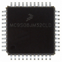
MC9S08JM32CLD Freescale Semiconductor, MC9S08JM32CLD Datasheet - Page 83

MC9S08JM32CLD
Manufacturer Part Number
MC9S08JM32CLD
Description
IC MCU 8BIT 32K FLASH 44-LQFP
Manufacturer
Freescale Semiconductor
Series
HCS08r
Datasheet
1.MC9S08JM32CLD.pdf
(388 pages)
Specifications of MC9S08JM32CLD
Core Processor
HCS08
Core Size
8-Bit
Speed
48MHz
Connectivity
I²C, LIN, SCI, SPI, USB
Peripherals
LVD, POR, PWM, WDT
Number Of I /o
33
Program Memory Size
32KB (32K x 8)
Program Memory Type
FLASH
Ram Size
2K x 8
Voltage - Supply (vcc/vdd)
2.7 V ~ 5.5 V
Data Converters
A/D 8x12b
Oscillator Type
External
Operating Temperature
-40°C ~ 85°C
Package / Case
44-LQFP
Processor Series
S08JM
Core
HCS08
Data Bus Width
8 bit
Data Ram Size
2 KB
Interface Type
SCI/SPI
Maximum Clock Frequency
24 MHz
Number Of Programmable I/os
33
Number Of Timers
8
Maximum Operating Temperature
+ 85 C
Mounting Style
SMD/SMT
3rd Party Development Tools
EWS08
Development Tools By Supplier
DEMOJM, DEMOJMSKT, DEMOFLEXISJMSD, DEMO9S08JM16
Minimum Operating Temperature
- 40 C
On-chip Adc
8-ch x 12-bit
Lead Free Status / RoHS Status
Lead free / RoHS Compliant
Eeprom Size
-
Lead Free Status / Rohs Status
Lead free / RoHS Compliant
Available stocks
Company
Part Number
Manufacturer
Quantity
Price
Company:
Part Number:
MC9S08JM32CLD
Manufacturer:
Freescale Semiconductor
Quantity:
1 948
Company:
Part Number:
MC9S08JM32CLD
Manufacturer:
Freescale Semiconductor
Quantity:
10 000
- Current page: 83 of 388
- Download datasheet (5Mb)
6.3.1
An internal pullup device can be enabled for each port pin by setting the corresponding bit in one of the
pullup enable registers (PTxPEn). The pullup device is disabled if the pin is configured as an output by the
parallel I/O control logic or any shared peripheral function regardless of the state of the corresponding
pullup enable register bit. The pullup device is also disabled if the pin is controlled by an analog function.
6.3.2
Slew rate control can be enabled for each port pin by setting the corresponding bit in one of the slew rate
control registers (PTxSEn). When enabled, slew control limits the rate at which an output can transition in
order to reduce EMC emissions. Slew rate control has no effect on pins which are configured as inputs.
6.3.3
An output pin can be selected to have high output drive strength by setting the corresponding bit in one of
the drive strength select registers (PTxDSn). When high drive is selected a pin is capable of sourcing and
sinking greater current. Even though every I/O pin can be selected as high drive, the user must ensure that
the total current source and sink limits for the chip are not exceeded. Drive strength selection is intended
to affect the DC behavior of I/O pins. However, the AC behavior is also affected. High drive allows a pin
to drive a greater load with the same switching speed as a low drive enabled pin into a smaller load.
Because of this the EMC emissions may be affected by enabling pins as high drive.
6.4
Depending on the stop mode, I/O functions differently as the result of executing a STOP instruction. An
explanation of I/O behavior for the various stop modes follows:
6.5
This section provides information about the registers associated with the parallel I/O ports and pin control
functions. These parallel I/O registers are located in page zero of the memory map and the pin control
registers are located in the high page register section of memory.
Freescale Semiconductor
•
•
Stop2 mode is a partial power-down mode, whereby I/O latches are maintained in their state as
before the STOP instruction was executed. CPU register status and the state of I/O registers must
be saved in RAM before the STOP instruction is executed to place the MCU in stop2 mode. Upon
recovery from stop2 mode, before accessing any I/O, the user must examine the state of the PPDF
bit in the SPMSC2 register. If the PPDF bit is 0, I/O must be initialized as if a power on reset had
occurred. If the PPDF bit is 1, I/O data previously stored in RAM, before the STOP instruction was
executed, peripherals may require being initialized and restored to their pre-stop condition. The
user must then write a 1 to the PPDACK bit in the SPMSC2 register. Access to I/O is now permitted
again in the user’s application program.
In stop3 mode, all I/O is maintained because internal logic circuity stays powered up. Upon
recovery, normal I/O function is available to the user.
Pin Behavior in Stop Modes
Parallel I/O and Pin Control Registers
Internal Pullup Enable
Output Slew Rate Control Enable
Output Drive Strength Select
MC9S08JM60 Series Data Sheet, Rev. 3
Chapter 6 Parallel Input/Output
83
Related parts for MC9S08JM32CLD
Image
Part Number
Description
Manufacturer
Datasheet
Request
R
Part Number:
Description:
Manufacturer:
Freescale Semiconductor, Inc
Datasheet:
Part Number:
Description:
Manufacturer:
Freescale Semiconductor, Inc
Datasheet:
Part Number:
Description:
Manufacturer:
Freescale Semiconductor, Inc
Datasheet:
Part Number:
Description:
Manufacturer:
Freescale Semiconductor, Inc
Datasheet:
Part Number:
Description:
Manufacturer:
Freescale Semiconductor, Inc
Datasheet:
Part Number:
Description:
Manufacturer:
Freescale Semiconductor, Inc
Datasheet:
Part Number:
Description:
Manufacturer:
Freescale Semiconductor, Inc
Datasheet:
Part Number:
Description:
Manufacturer:
Freescale Semiconductor, Inc
Datasheet:
Part Number:
Description:
Manufacturer:
Freescale Semiconductor, Inc
Datasheet:
Part Number:
Description:
Manufacturer:
Freescale Semiconductor, Inc
Datasheet:
Part Number:
Description:
Manufacturer:
Freescale Semiconductor, Inc
Datasheet:
Part Number:
Description:
Manufacturer:
Freescale Semiconductor, Inc
Datasheet:
Part Number:
Description:
Manufacturer:
Freescale Semiconductor, Inc
Datasheet:
Part Number:
Description:
Manufacturer:
Freescale Semiconductor, Inc
Datasheet:
Part Number:
Description:
Manufacturer:
Freescale Semiconductor, Inc
Datasheet:


